SSZTB52 july 2016 LMG5200 , TPS53632G
Enterprise server, switch, base station and storage hardware designers are always looking to increase power density and efficiency on their motherboards. With the addition of more components on the motherboard and a shrinking form factor, power-supply density becomes the limiting factor in reducing the area further. The smaller the power supply, the smaller the motherboard and reducing motherboard size enables fitting more boards into a given rack to maximize data-center throughput and performance.
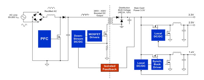
In the typical telecom power-supply system shown in Figure 1, the 48VDC input voltage has to be further stepped down to an intermediate bus voltage (3.3V in this case) which one or more buck direct current (DC/DC) converters then take and step down to various regulated lower-output voltages needed for processor, ASIC, and FPGA core rail voltages, I/O rails, DDR memory, PHY chips and other low-voltage components.
 Figure 1 An Alternating Current (AC) to
48V to Point-of-load (POL) Telecom Power System
Figure 1 An Alternating Current (AC) to
48V to Point-of-load (POL) Telecom Power SystemTI’s gallium nitride (GaN) DC/DC solutions eliminate the intermediate bus DC/DC conversion stage so that designers can step 48V down to lower output voltages in a single stage.
Eliminating the intermediate bus DC/DC converter enables significant increases in power density and system cost, with an accompanying increase in reliability.
GaN’s advantages over silicon MOSFETs include:
- Low input and output capacitance to reduce switching losses and enable faster switching frequencies.
- Near-zero reverse-recovery charge for no reverse-recovery losses and reduced losses in Class-D inverters/amplifiers.
- Greatly reduced switching losses due to lower gate-drain capacitance, enabling higher switching frequencies and reducing or even eliminating heat sinks.
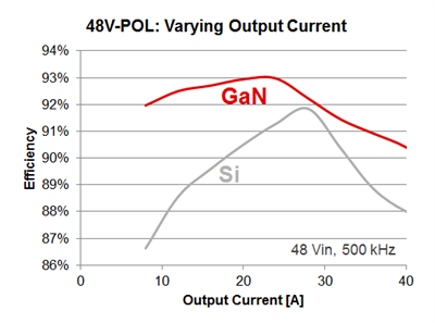
Figure 2 shows a 48V-to-POL efficiency comparison between GaN and silicon FETs.
 Figure 2 48V-to-POL GaN vs. Silicon
DC/DC Converter Efficiency with Varying Load Current
Figure 2 48V-to-POL GaN vs. Silicon
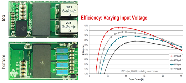
DC/DC Converter Efficiency with Varying Load CurrentTI’s new 48V-to-POL GaN single-stage solution – using the TPS53632G driverless pulse-width modulation (PWM) controller and LMG5200 80V GaN half-bridge power stage (drivers and GaN FETs in one integrated circuit) – enables high power density, fast load-transient response, high efficiency, excellent thermal performance and increased system reliability in a total area of ~700mm2 for 48W of output power. Efficiency is ~88% at 48V with 60V input, 1V output, 50A and a 600kHz switching frequency, as shown in Figure 3.
Module efficiency peaks at ~91% and is still ~90% at 35A of output current. Notably, efficiency does not significantly drop even when increasing the input voltage to 75V.
 Figure 3 48V-to-POL GaN DC/DC Converter
Reference Design and Efficiency with Varying Load Current at 600KHz
Figure 3 48V-to-POL GaN DC/DC Converter
Reference Design and Efficiency with Varying Load Current at 600KHzIf you are designing 48V-to-POL DC/DC converters for end applications such as enterprise servers, switches, base stations and storage and have traditionally used 48V-to-intermediate bus and intermediate bus-to-POL DC/DC converters, it’s time to simplify your design and increase power density and reliability with TI’s GaN DC/DC solutions. Check out TI’s complete GaN DC/DC conversion portfolio on the GaN Solutions portal.