SSZTC74 september 2015 LMG5200
Guest blogger Jan Cumps is an active E2E community member, showcasing some of the best projects from around the TI Community
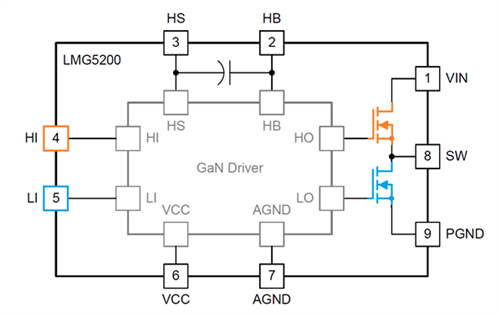
The rise of discrete gallium nitride (GaN) FETs has increased the need for more user-friendly interfaces while also improving efficiency. Half-bridge GaN power stages such as the LMG5200 have a separate drive input for the high and low GaN FET. The two inputs (pin 4 and 5 in Figure 1) give you the ability to optimize efficiency because you can tweak the exact point at which each FET switches on and off.
But this option also comes with responsibilities. To prevent shoot-through during switching between the FETs, you have to provide a dead time between the switching off of one FET and the switching on of the other.
That’s why you shouldn't just use a pulse-width modulation (PWM) signal and its inverse to drive the high and low inputs, because you have to generate a wait time between the falling edge of one input and the rising edge of the other (Figure 2).
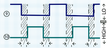 Figure 2 Inverted Driver Input Signals
with Dead Time Delay
Figure 2 Inverted Driver Input Signals
with Dead Time DelayThe evaluation board for the LMG5200 GaN half-bridge power stage uses the classic time-delay circuit to generate this tiny delay. Fans of the iconic book, “The Art of Electronics,” will recognize the setup as one of the practical examples from the first chapter. While the example given in the book generates a delay on both edges of a square wave, TI designers adapted the board so that it only inserts the delay on the rising edges. And that’s exactly the behavior you need.
The Dead-time Generator Schematics
The user’s guide documents the full schematics of the evaluation board. Figure 3 shows the module that generates the high and low drive signals with the dead time.
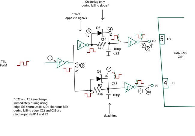 Figure 3 Dead Time Generator
Schematic
Figure 3 Dead Time Generator
SchematicIf you abstract away the diodes, resistors and capacitors, the circuit generates an in-phase and an inverted signal from the PWM input. There will always be one side of the half bridge that’s on and one side that’s off. The passive components will generate that dead time for you, so let’s dig a little deeper into that part.
“The Art of Electronics”
In Chapter 1 of “The Art of Electronics,” the authors present a time-delay circuit. It uses an RC circuit – flanked by two complementary metal-oxide semiconductor (CMOS) buffers – to glue a short delay to both flanks of a PWM signal (Figure 4).
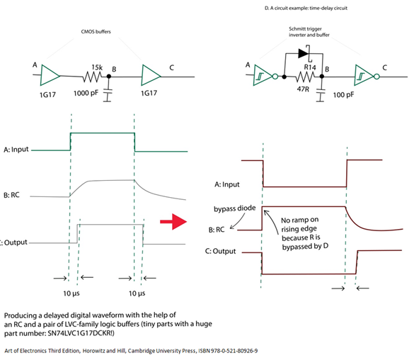 Figure 4 Comparison of Time-delay
Circuit from “Art of Electronics” and TI Asymmetric Delay Generator
Figure 4 Comparison of Time-delay
Circuit from “Art of Electronics” and TI Asymmetric Delay GeneratorIn TI's reference design, a fast-switching Schottky diode in parallel with the resistor bypasses the RC delay during one of the edges.
The High and Low Signals with Dead Time
Let's follow the HI signal path of the evaluation board schematics (D4, R2 and C35 in Figure 3). Diode D4 bypasses R2 during the falling edge of input A (signal 1 in Figure 3 and Figure 5). At the output of the first inverter (signal 6), this input signal’s falling edge becomes a rising edge. The diode conducts and the R component of the RC circuit is almost 0. The RC constant is also almost 0. So the circuit adds virtually no delay to that flank (signal 7). After the second inverter, this becomes a falling flank again (signals 8 and 10).
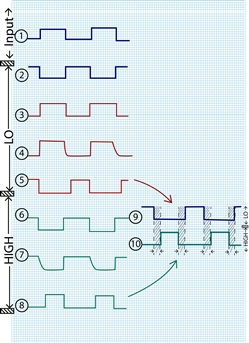 Figure 5 Signal Transformation from
Simple Input to Inverted Outputs with Dead Time
Figure 5 Signal Transformation from
Simple Input to Inverted Outputs with Dead TimeWhen the input signal rises (again at signal 1), the signal after the inverter becomes a falling edge (signal 6). The diode D4 blocks and leaves R2 alone. You get a real RC circuit with 47Ω and 100pF. That will turn the edge into a ramp (signal 7). The Schmitt trigger front end of the second inverter will ensure that the output signal flips at a predictable voltage (and at a predictable time). So the result is that the rising edge at the output (signals 8 and 10) will lag compared to the input signal. And that was the effect I was after.
The LO signal path does exactly the same. An additional inverter at the input of this path ensures that both sides see and process an opposite signal: one to drive the high-side FET and one to drive the low-side FET. As a result, you’ll get two related signals, as shown in Figure 2. A signal only turns high after the other one switches off, and after that dead time has passed, which was our ultimate goal.
Figure 6 shows the capture of both inputs of the LMG5200 at the two transitions.
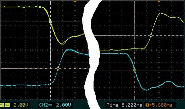 Figure 6 Capture of HI-LO and LO-HI
Transition of Both Driver Signals.
Figure 6 Capture of HI-LO and LO-HI
Transition of Both Driver Signals.You can vary the duty cycle and the frequency of the input signal as required. The dead time will stay constant.
By using a classic time delay circuit, you can safely drive a GaN half-bridge power stage with a simple PWM signal and control its output with variable duty cycle. What is your approach to generate dead times in your switching applications?
