SWRU550A February 2019 – May 2019
6.4 PCB Layout Recommendations
An important consideration when doing the layout is the trace width for the Ethernet and USB signals. The Ethernet and USB interfaces have critical differential impedance requirements. Both Ethernet signal pairs must be routed as a 100 Ω ± 10% differential pair on the top layer of the PCB with a ground plane as a reference. The USB signal pair must be routed as a 90 Ω ± 10% differential pair on the top layer of the PCB with a ground plane as a reference.
The optimal solution is if the PCB fab house adjusts the stack up and provides for controlled dielectric. The PCB tools must be used to set the spacing and width of the traces to get close to the target characteristic impedance. The PCB fab house can then adjust the trace space and width to the specific materials and process.
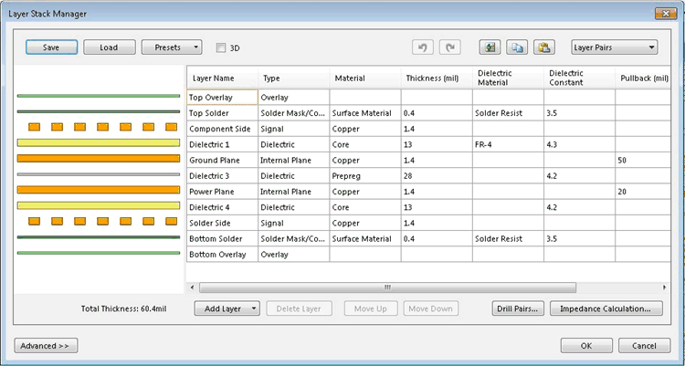
During the PCB layout, if the PCB fab house has a predefined layer stack up for low-cost process, the layer stack up information must be found and used in PCB tools to get the optimum trace width. The design files use a low cost variant with the following PCB stack up for four layer PCB’s.
Figure 6 shows the PCB layer stack up for TIDM-1018.
 Figure 6. PCB Layer Stack Up for TIDM-1018
 When the data shown in Figure 6 is entered into the PCB tool, the trace width and space for Ethernet and USB signals are computed and listed in Table 4. The most important parameter is the ZDIFF, which must be within ±10% tolerance.
Table 4. Differential Signals Trace Information
| Trace Width
(mil) |
Trace Thickness
(mil) |
Trace Height
(mil) |
Trace Spacing
(mil) |
ER | ZDIFF | ZO |
|---|---|---|---|---|---|---|
| 10 | 0.4 | 15.8 | 5 | 4.2 | 109.476 | 84.766 |
| 12.8 | 0.4 | 15.8 | 5 | 4.2 | 99.336 | 76.915 |