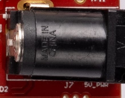
SWRU620 April   2024


  1.   1
  2.   Description
  3.   Features
  4.   Applications
  5.   5
  6. 1Evaluation Module Overview
    1. 1.1 Introduction
    2. 1.2 Kit Contents
    3. 1.3 Specification
      1. 1.3.1 Block Diagram
      2. 1.3.2 EVM Mux Block Diagram
    4. 1.4 Device Information
    5. 1.5 xWRL6432AOPEVM Antenna
  7. 2Hardware
    1. 2.1 PCB Material
    2. 2.2 Switches and LEDs
      1. 2.2.1 SOP Configuration
      2. 2.2.2 Switches
    3. 2.3 DC Jack
    4. 2.4 DCA1000 HD Connector
    5. 2.5 CANFD Connector
    6. 2.6 LIN PHY Connection
    7. 2.7 I2C Connections
      1. 2.7.1 EEPROM
      2. 2.7.2 On-Board Sensors
    8. 2.8 XDS110 Interface
    9. 2.9 FTDI Interface
  8. 3Software
    1. 3.1 Software Description
    2. 3.2 Flashing the Board
    3. 3.3 mmWave Out of Box Demo
      1. 3.3.1 XWRL6432AOP Demo Visualization Getting Started
    4. 3.4 DCA1000EVM Mode
  9. 4Hardware Design Files
    1. 4.1 Schematics
    2. 4.2 PCB Layouts
      1. 4.2.1 PCB Storage and Handling Recommendations:
        1. 4.2.1.1 PCB Storage and Handling Recommendations:
        2. 4.2.1.2 Higher Power Demanding Applications
    3. 4.3 Bill of Materials (BOM)
  10. 5Additional Information
    1. 5.1 Trademarks
  11. 6Related Documentation
  12. 7TI E2E Community
  13. 8References

DC Jack

Higher current support: When using the EVM with the external power adapter, the 5V supply is provided by the external power adapter. For most of the use cases, this external power supply option is not used, as power is derived from the USB interface.

GUID-E08160BC-0B30-4A98-91D6-E146E41E6804-low.jpg
Note: After the 5V power supply is provided to the EVM, TI recommends pressing the NRST switch one time to verify a reliable boot-up state.
Note: All digital IO pins of the device (except NRESET) are not fail safe; hence, care needs to be taken that the pins are not driven externally without the VIO supply being present to the device.