TIDU312A May 2014 – November 2020
- Trademarks
- 1Introduction
- 2Software Overview
- 3Procedure for Running the Incremental Builds
- 4Test Results
- 5References
- 6Revision History
3.1.2 Build 1 Overview
The software in Build1 has been configured so that the user can quickly evaluate the PWM driver module by viewing the related waveforms on a scope and observing the effect of duty cycle change on PFC output voltage. The user can adjust the PWM duty cycle from CCS watch window. The user can also evaluate the ADC driver module by viewing the ADC sampled data in the watch window.
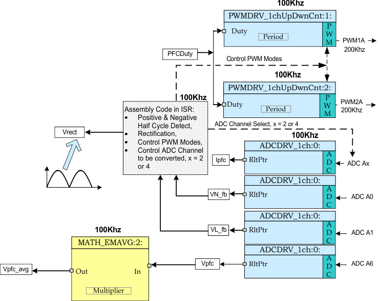
The PWM and ADC driver macro instantiations are executed inside the _DPL_ISR. Figure 3-1 shows the software blocks used in this build. The two PWM signals for the two PFC switches are obtained from ePWM module 1 & 2. ePWM1A drives one of the PFC switches while ePWM2A drives the other.
The quantities that are sensed and fed back to the MCU include, (1) the line and neutral voltages (VL_fb, VN_fb), (2) the two PFC switch currents (Isw1, Isw2) each sampled at appropriate line half cycle and then saved as Ipfc, and (3) the DC bus voltage (Vpfc). These quantities are read using the ADC driver module and are indicated in Figure 3-1. The ADC driver module converts the 12-bit ADC result to a 32bit Q24 value. A few lines of code in the ISR implements the detection of input AC line half cycle (positive and negative half cycles) and the selection of the appropriate PFC switch current as Ipfc. These lines of code also configures the appropriate PWM output (PWM1A, PWM2A) to operate either in PWM mode or in forced ON mode depending on the input AC line half cycle.
 Figure 3-1 Build 1 Software
Blocks
Figure 3-1 Build 1 Software
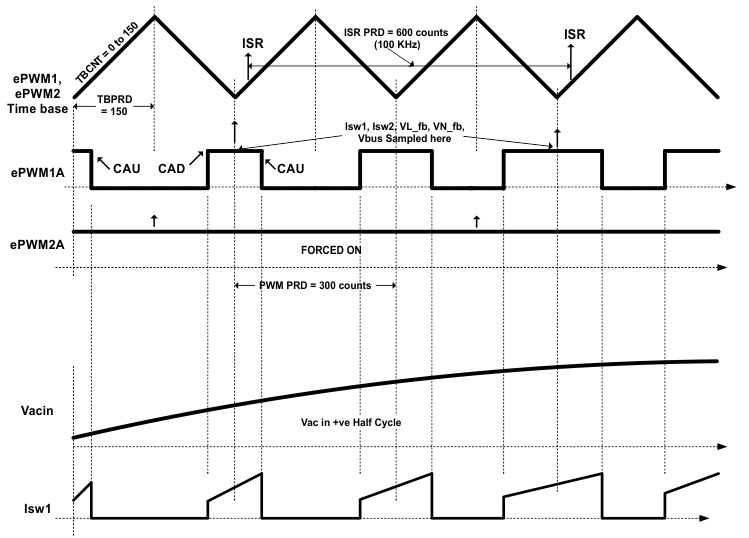
BlocksThe PWM signals are generated at a frequency of 200 kHz, such that, a period of 5 μs. With the controller operating at 60 MHz, one count of the time base counter of ePWM1 corresponds to 16.6667 ns. This implies a PWM period of 5 μs is equivalent to 300 counts of the time base counter (TBCNT1, TBCNT2). The ePWM1 and ePWM2 modules are configured to operate in up-down count mode as shown in Figure 3-2. This means a time base period value of 150 (period register value) will give a total PWM period value of 300 counts (5 μs).
PFC switch current is sampled at the midpoint of the PWM ON pulse since the sampled value represents the average inductor current under CCM (continuous conduction mode) condition. Under DCM condition this sampled switch current value also represents a fraction of the average inductor current. This relationship between the sampled switch current and average inductor current can be derived by analyzing the related waveforms under DCM and CCM condition.
All the other voltage signal conversion is also initiated at this time. This is indicated in Figure 3-2. The flexibility of ADC and PWM modules on C2000 devices allow for precise and flexible ADC start of conversions. In this case ePWM1 is used as a time base to generate a start of conversion (SOC) trigger when the TBCNT1 reaches zero. A dummy ADC conversion is performed at this point in order to ensure the integrity of the ADC results.
Figure 3-2 also shows the PWM outputs when the input AC voltage is in positive half cycle. Corresponding switch current Isw1 is also shown as the current converted and saved as Ipfc for PFC current loop control.
 Figure 3-2 PWM
Generation and ADC Sampling
Figure 3-2 PWM
Generation and ADC SamplingOn a CAU event (TBCNT1 = CMPA and counting up), ePWM1A output is Reset, while on a CAD event (TBCNT1 = CMPA and counting down), ePWM1A output is Set. ePWM2A is set to forced ON mode. This configuration of ePWM1A and ePWM2A happens during the positive half cycle of the input voltage. For negative half cycle of input voltage the two PWM output configurations are switched, ePWM1A goes into forced ON mode and ePWM2A runs in PWM mode.
The CMPA value is derived from the input “PFCDuty” (Q24 variable) command.
Table 3-1 gives example CMPA values calculated for a TBPRD value of 150.
| PFCDuty (Hex Values in Q24) |
CMPA = (PFCDuty/(224-1))*TBPRD | % Duty |
|---|---|---|
| 0x00200000 | 18 | 12.5 |
| 0x00800000 | 75 | 50 |
| 0x00FFFFFF | 150 | 100 |
The ADC module is configured to use SOCA of ePWM1 such that, SOCA is triggered at TBCNT1 = ZERO event. All conversions are completed using this SOCA trigger. These 5 ADC results are read in the ISR by executing the ADC driver module from the 100 kHz ISR labeled as _DPL_ISR.
This ISR in assembly (_DPL_ISR) is triggered by EPWM1 on a CMPB match event on up count. CMPB is set to 80 so that the ISR is triggered only after the ADC conversions are complete. This is where the PWMDRV_1ch_UpDwnCnt macros are executed and the PWM compare shadow registers updated. These are loaded in to the active register at the next TBCNT = ZERO event. Note that the ISR trigger frequency is half that of the PWM switching frequency as shown in Figure 3-2.