TIDUD61E October   2020  – April 2021


  1.   Description
  2.   Resources
  3.   Features
  4.   Applications
  5.   5
  6. 1System Description
    1. 1.1 Key System Specifications
  7. 2System Overview
    1. 2.1 Block Diagram
    2. 2.2 Design Considerations
      1. 2.2.1 Input AC Voltage Sensing
      2. 2.2.2 Bus Voltage Sensing
      3. 2.2.3 AC Current Sensing
      4. 2.2.4 Sense Filter
      5. 2.2.5 Protection (CMPSS)
    3. 2.3 Highlighted Products
      1. 2.3.1 C2000™ MCU F28004x
      2. 2.3.2 LMG3410R070
      3. 2.3.3 UCC27714
    4. 2.4 System Design Theory
      1. 2.4.1 PWM
      2. 2.4.2 Current Loop Model (PFC and Inverter mode)
      3. 2.4.3 DC Bus Regulation Loop (for PFC mode only)
      4. 2.4.4 Soft Start Around Zero Crossing for Eliminate or Reduce Current Spike
      5. 2.4.5 AC Drop Test
  8. 3Hardware, Software, Testing Requirements, and Test Results
    1. 3.1 Required Hardware and Software
      1. 3.1.1 Hardware
        1. 3.1.1.1 Base Board Settings
        2. 3.1.1.2 Control Card Settings
      2. 3.1.2 Software
        1. 3.1.2.1 Opening Project Inside CCS
        2. 3.1.2.2 Project Structure
        3. 3.1.2.3 Using CLA on C2000 MCU to Alleviate CPU Burden
        4. 3.1.2.4 CPU and CLA Utilization and Memory Allocation
        5. 3.1.2.5 Running the Project
          1. 3.1.2.5.1 Lab 1: Open Loop, DC (PFC Mode)
            1. 3.1.2.5.1.1 Setting Software Options for LAB 1
            2. 3.1.2.5.1.2 Building and Loading Project
            3. 3.1.2.5.1.3 Setup Debug Environment Windows
            4. 3.1.2.5.1.4 Using Real-Time Emulation
            5. 3.1.2.5.1.5 Running Code
          2. 3.1.2.5.2 Lab 2: Closed Current Loop DC (PFC)
            1. 3.1.2.5.2.1 Setting Software Options for Lab 2
            2. 3.1.2.5.2.2 Designing Current Loop Compensator
            3. 3.1.2.5.2.3 Building and Loading Project and Setting up Debug
            4. 3.1.2.5.2.4 Running Code
          3. 3.1.2.5.3 Lab 3: Closed Current Loop, AC (PFC)
            1. 3.1.2.5.3.1 Setting Software Options for Lab 3
            2. 3.1.2.5.3.2 Building and Loading Project and Setting up Debug
            3. 3.1.2.5.3.3 Running Code
          4. 3.1.2.5.4 Lab 4: Closed Voltage and Current Loop (PFC)
            1. 3.1.2.5.4.1 Setting Software Options for Lab 4
            2. 3.1.2.5.4.2 Designing Voltage Loop Compensator
            3. 3.1.2.5.4.3 Building and Loading Project and Setting up Debug
            4. 3.1.2.5.4.4 Running Code
          5. 3.1.2.5.5 Lab 5: Open loop, DC (Inverter)
            1. 3.1.2.5.5.1 Setting Software Options for Lab 5
            2. 3.1.2.5.5.2 Building and Loading Project
            3. 3.1.2.5.5.3 Setup Debug Environment Windows
            4. 3.1.2.5.5.4 Running Code
          6. 3.1.2.5.6 Lab 6: Open loop, AC (Inverter)
            1. 3.1.2.5.6.1 Setting Software Options for Lab 6
            2. 3.1.2.5.6.2 Building and Loading Project and Setting up Debug
            3. 3.1.2.5.6.3 Running Code
          7. 3.1.2.5.7 Lab 7: Closed Current Loop, DC (Inverter with resistive load)
            1. 3.1.2.5.7.1 Setting Software Options for Lab 7
            2. 3.1.2.5.7.2 Designing Current Loop Compensator
            3. 3.1.2.5.7.3 Building and Loading Project and Setting up Debug
            4. 3.1.2.5.7.4 Running Code
          8. 3.1.2.5.8 Lab 8: Closed Current Loop, AC (Inverter with resistive load)
            1. 3.1.2.5.8.1 Setting Software Options for Lab 8
            2. 3.1.2.5.8.2 Building and Loading Project and Setting up Debug
            3. 3.1.2.5.8.3 Running Code
          9. 3.1.2.5.9 Lab 9: Closed Current Loop (Grid Connected Inverter)
            1. 3.1.2.5.9.1 Setting Software Options for Lab 9
            2. 3.1.2.5.9.2 Building and Loading Project and Setting up Debug
            3. 3.1.2.5.9.3 Running Code: Emulated Grid-tied Condition (Verification purpose only)
            4. 3.1.2.5.9.4 Running Code: Grid-tied Condition
        6. 3.1.2.6 Running Code on CLA
        7. 3.1.2.7 Advanced Options
          1. 3.1.2.7.1 Input Cap Compensation for PF Improvement Under Light Load
          2. 3.1.2.7.2 83
          3. 3.1.2.7.3 Adaptive Dead Time for Efficiency Improvements
          4. 3.1.2.7.4 Phase Shedding for Efficiency Improvements
          5. 3.1.2.7.5 Non-Linear Voltage Loop for Transient Reduction
          6. 3.1.2.7.6 Software Phase Locked Loop Methods: SOGI - FLL
    2. 3.2 Testing and Results
      1. 3.2.1 Test Results at Input 120 Vrms, 60 Hz, Output 380-V DC
        1. 3.2.1.1 Startup
        2. 3.2.1.2 Steady State Condition
        3. 3.2.1.3 Transient Test With Step Load Change
          1. 3.2.1.3.1 0% to 50% Load Step Change
          2. 3.2.1.3.2 50% to 100% Load Step Change
          3. 3.2.1.3.3 100% to 50% Load Step Change
          4. 3.2.1.3.4 50% to 100% Load Step Change
      2. 3.2.2 Test Results at Input 230 Vrms, 50 Hz, Output 380 V DC
        1. 3.2.2.1 Startup
        2. 3.2.2.2 Steady State Condition
        3. 3.2.2.3 Transient Test With Step Load Change
          1. 3.2.2.3.1 33% to 100% Load Step Change
          2. 3.2.2.3.2 100% to 33% Load Step Change
      3. 3.2.3 Test Results Graphs
  9. 4Design Files
    1. 4.1 Schematics
    2. 4.2 Bill of Materials
    3. 4.3 PCB Layout Recommendations
      1. 4.3.1 Layout Prints
    4. 4.4 Altium Project
    5. 4.5 Gerber Files
    6. 4.6 Assembly Drawings
  10. 5Software Files
  11. 6Related Documentation
    1. 6.1 Trademarks
  12. 7About the Author
  13. 8Revision History
Running Code: Emulated Grid-tied Condition (Verification purpose only)
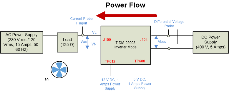
GUID-56A5F797-A295-4499-9E65-2F8F542529E4-low.gifFigure 3-40 HW setup for Build 6 Emulated Grid Condition
  1. The project is programmed to wait for dc bus voltage and ac source voltage to exceed approximately 340 V and 75 Vrms to drive the in rush relay, and clear the trip.
  2. Run the project by clicking GUID-0E577519-64C9-4C89-A28C-975CCF35D80F-low.png.
  3. Now apply an input voltage of approximately 340 V, the board comes out of the undervoltage condition. To run the solution, ac voltage in the output of the inverter has to be higher than 75 V rms and then inrush relay is driven. TTPLPFC_ac_cur_ref is set to -0.03 by default.
  4. Change TTPLPFC_pwmSwState from pwmSwState_defaultState to pwmSwState_normalOperation to enable pwm output. The pwm output is turned off by default and the inverter does not work without selecting this option.
  5. Slowly increase TTPLPFC_ac_cur_ref to -0.05 and inverter output current is close to 0.8 A in RMS value. The output voltage of the inverter is determined by the ac voltage source.
  6. As the source impedance of the emulgated grid condition is not as small as the actual grid, the bandwidth of the current loop is much lower than the designed target and the system suffers from huge current spikes near zero crossing.
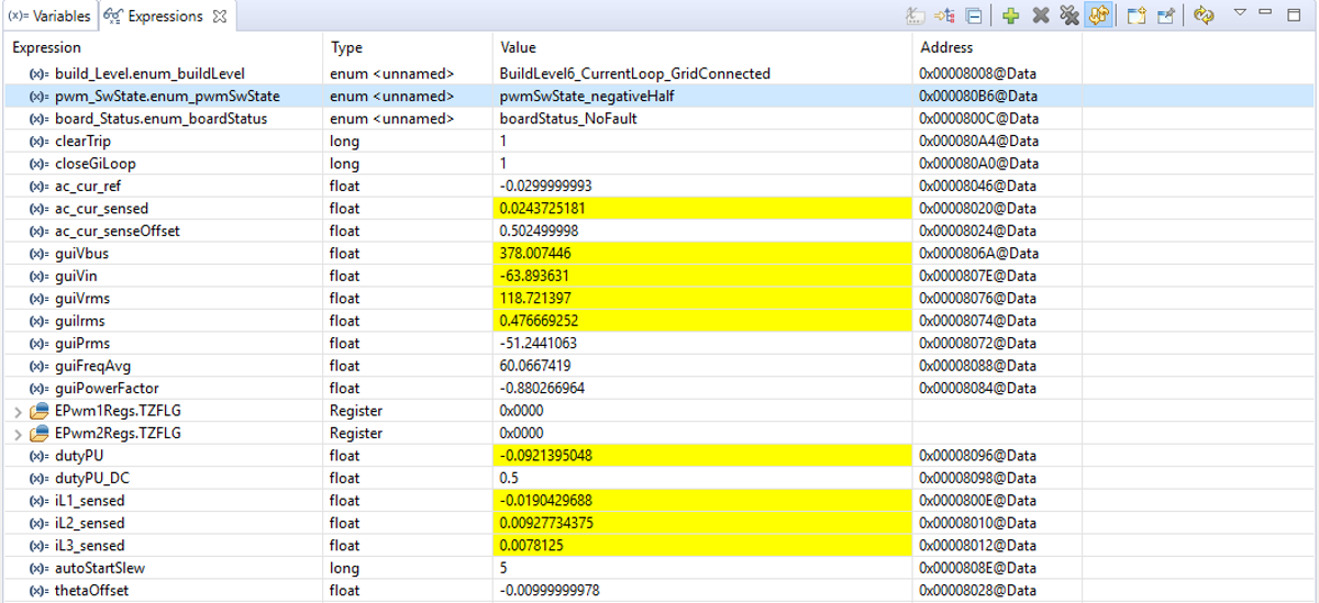
    GUID-1B88C913-A524-40A8-9A24-1934B4A7D44A-low.pngFigure 3-41 Lab 9: Closed Current Loop after close the current loop
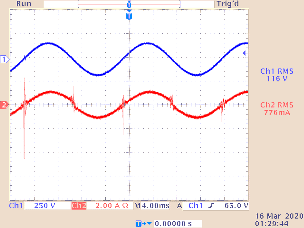
    GUID-55E16EC9-328F-4B67-8B1B-3FA260034A51-low.pngFigure 3-42 Voltage and current waveform (Lab 9 Emulated Grid Condition)
  7. To bring the system to a safe stop, switch off the output from the AC power supply first and switch off the input DC power supply subsequently. This will eliminate the risk of the undesired reverse power flow in the inverter mode. Bring input AC voltage down to zero and observe the TTPLPFC_ac_volRms_sensed_Volts comes down to zero as well. After AC voltage is fully switched off, the the input DC voltage has to be down to zero, observe the TTPLPFC_vBus_sensed_Volts becomes zero.
  8. Fully halting the MCU when in real-time mode is a two-step process. First halt the processor by using the Halt button on the toolbar (GUID-CEC61420-51B7-45ED-A276-0E2E645982AD-low.png) or by using TargetHalt. Then take the MCU out of real-time mode by clicking on GUID-F443C7B8-178A-4910-9044-9BC0FA9477F3-low.png. Finally, reset the MCU (GUID-8E8358D6-E5B2-4960-9A30-90C9B77C035B-low.png) .
  9. Close the CCS debug session by clicking Terminate Debug Session (TargetTerminate all).
    GUID-38039C67-CB5D-4301-8BC2-3B268FD4BD48-low.png