TIDUED7A November   2018  – November 2022


  1.   Description
  2.   Resources
  3.   Features
  4.   Applications
  5.   5
  6. 1System Description
    1. 1.1 Key System Specifications
  7. 2System Overview
    1. 2.1 Block Diagram
    2. 2.2 Highlighted Products
      1. 2.2.1 LM5155-Q1
      2. 2.2.2 TPS92610-Q1, TPS92611-Q1
    3. 2.3 System Design Theory
      1. 2.3.1  PCB and Form Factor
      2. 2.3.2  Input Protection
      3. 2.3.3  EMI Filter
      4. 2.3.4  LM5155-Q1 Voltage Regulator
      5. 2.3.5  Tail Light (2x TPS92611-Q1)
      6. 2.3.6  Stop Light (2x TPS92610-Q1)
      7. 2.3.7  Turn Light (TPS92610-Q1)
      8. 2.3.8  Backup Light
      9. 2.3.9  Enabling Light Functions
      10. 2.3.10 Diagnostic
      11. 2.3.11 LED Load
  8. 3Hardware, Software, Testing Requirements, and Test Results
    1. 3.1 Required Hardware
    2. 3.2 Testing and Results
      1. 3.2.1 Startup / Shutdown
      2. 3.2.2 Steady State Operation
      3. 3.2.3 Load Transient Response
      4. 3.2.4 Stability
      5. 3.2.5 Efficiency
      6. 3.2.6 Electromagnetic Compatibility (EMC)
        1. 3.2.6.1 Conducted Emissions
        2. 3.2.6.2 Radiated Emissions
      7. 3.2.7 Thermal Performance
  9. 4Design Files
    1. 4.1 Schematics
    2. 4.2 Bill of Materials
    3. 4.3 PCB Layout Recommendations
      1. 4.3.1 Layout Prints
    4. 4.4 Altium Project
    5. 4.5 Gerber Files
    6. 4.6 Assembly Drawings
  10. 5Related Documentation
  11. 6Trademarks
  12. 7About the Author
  13. 8Revision History

LM5155-Q1

The LM5155x device is a wide-input range, non-synchronous boost controller which employs peak current mode control. The device is suitable for use in boost, SEPIC, and flyback topologies.

The wide input range of the device covers automotive cold crank and load dump transient. The device can start up from a 1-cell battery with a minimum 2.97 V. After start-up, the device can operate down to 1.5-V input by supplying the BIAS pin from the boost converter output. The switching frequency is programmed with an external resistor from 100 kHz to 2.2 MHz. Switching at 2.2 MHz minimizes AM band interference and allows for a small solution size and fast transient response.

The device features a 1.5-A standard MOSFET driver and a low, 100-mV current limit threshold. The device supports use of an external VCC supply to improve efficiency. In addition, low operating current and pulse skipping operation improve efficiency at light load.

The device has built-in protection features such as cycle-by-cycle current limit, over voltage protection, line UVLO, thermal shutdown and hiccup mode overload protection (LM51551). Additional features include low shutdown IQ, programmable soft start, programmable slope compensation, precision reference, power good indicator and external clock synchronization.
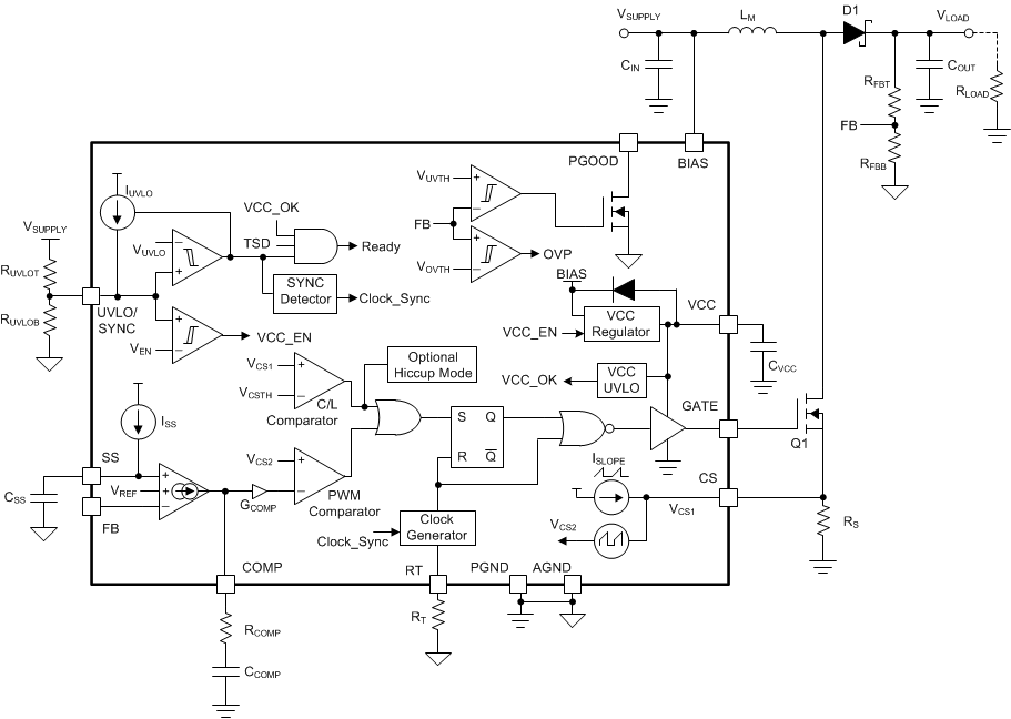
GUID-3698DDB5-A469-4406-AFD2-5437E1546269-low.gifFigure 2-2 Functional Block Diagram of the LM5155-Q1