SNVS247E September 2003 – August 2016 LP3875-ADJ
PRODUCTION DATA.
- 1 Features
- 2 Applications
- 3 Description
- 4 Revision History
- 5 Pin Configuration and Functions
- 6 Specifications
- 7 Detailed Description
-
8 Application and Implementation
- 8.1 Application Information
- 8.2
Typical Application
- 8.2.1 Design Requirements
- 8.2.2
Detailed Design Procedure
- 8.2.2.1 External Capacitors
- 8.2.2.2 CFF (Feed Forward Capacitor)
- 8.2.2.3 Selecting a Capacitor
- 8.2.2.4 Capacitor Characteristics
- 8.2.2.5 Setting The Output Voltage
- 8.2.2.6 Turnon Characteristics for Output Voltages Programmed to 2 V or Less
- 8.2.2.7 RFI/EMI Susceptibility
- 8.2.2.8 Output Noise
- 8.2.2.9 Power Dissipation
- 8.2.2.10 Estimating Junction Temperature
- 8.2.3 Application Curves
- 9 Power Supply Recommendations
- 10Layout
- 11Device and Documentation Support
- 12Mechanical, Packaging, and Orderable Information
Package Options
Mechanical Data (Package|Pins)
Thermal pad, mechanical data (Package|Pins)
- KTT|5
Orderable Information
1 Features
- Input Voltage Range: 2.5 V to 7 V
- Ultra Low Dropout Voltage
- Low Ground Pin Current
- Load Regulation of 0.06%
- 10-nA Quiescent Current in Shutdown Mode
- Specified Output Current of 1.5-A DC
- Minimum Output Capacitor Requirements
- Overtemperature/Overcurrent Protection
- −40°C to +125°C Junction Temperature Range
- Available in DDPAK/TO-263 and SOT-223 Packages
2 Applications
- Microprocessor Power Supplies
- GTL, GTL+, BTL, and SSTL Bus Terminators
- Power Supplies for DSPs
- SCSI Terminator
- Post Regulators
- High Efficiency Linear Regulators
- Battery Chargers
- Other Battery-Powered Applications
3 Description
The LP3875-ADJ fast ultra-low-dropout LDO operates from a 2.5-V to 7-V input supply. This ultra-low-dropout LDO responds very quickly to step changes in load, which makes it suitable for low-voltage microprocessor applications. The LP3875-ADJ is developed on a CMOS process, which allows low quiescent-current operation independent of output load current. This CMOS process also allows the LP3875-ADJ to operate under extremely low dropout conditions.
- Dropout Voltage: Ultra-low-dropout voltage; typically 38 mV at 150-mA load current and 380 mV at 1.5-A load current.
- Ground Pin Current: Typically 6 mA at 1.5-A load current.
- Shutdown Mode: Typically 10-nA quiescent current when the SD pin is pulled low.
- Adjustable Output Voltage: The output voltage may be programmed via two external resistors.
Device Information(1)
| PART NUMBER | PACKAGE | BODY SIZE (NOM) |
|---|---|---|
| LP3875-ADJ | SOT-223 (5) | 6.50 mm × 3.56 mm |
| TO-263 (5) | 10.16 mm × 8.42 mm |
- For all available packages, see the orderable addendum at the end of the data sheet.
space
space
space
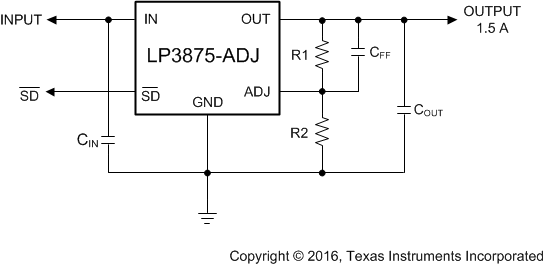
Simplified Schematic
