SCLS375F June 1997 – July 2014 SN74AHCT273
PRODUCTION DATA.
- 1 Features
- 2 Applications
- 3 Description
- 4 Simplified Schematics
- 5 Revision History
- 6 Pin Configuration and Functions
- 7 Specifications
- 8 Parameter Measurement Information
- 9 Detailed Description
- 10Application and Implementation
- 11Power Supply Recommendations
- 12Layout
- 13Device and Documentation Support
- 14Mechanical, Packaging, and Orderable Information
Package Options
Refer to the PDF data sheet for device specific package drawings
Mechanical Data (Package|Pins)
- DB|20
- NS|20
- N|20
- DW|20
- PW|20
Thermal pad, mechanical data (Package|Pins)
Orderable Information
1 Features
- Inputs are TTL-Voltage Compatible
- Contain Eight Flip-Flops With Single-Rail Outputs
- Direct Clear Input
- Individual Data Input to Each Flip-Flop
- Latch-Up Performance Exceeds 250 mA Per JESD 17
- ESD Protection Exceeds JESD 22
- 2000-V Human-Body Model (A114-A)
- 200-V Machine Model (A115-A)
- 1000-V Charged-Device Model (C101)
2 Applications
- Buffers and Storage Registers
- Shift Registers
- Pattern Generators
- Servers
- PCs and Notebooks
- Network Switches
- Memory Systems
- Databases
3 Description
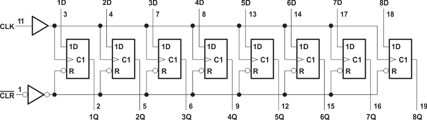
These devices are positive-edge-triggered D-type
flip-flops with a direct clear (CLR) input.
Device Information(1)
| PART NUMBER | PACKAGE | BODY SIZE (NOM) |
|---|---|---|
| SNx4AHCT273 | SSOP (20) | 7.20 mm × 5.30 mm |
| SOIC (20) | 12.80 mm × 7.50 mm | |
| PDIP (20) | 22.48 mm × 6.35 mm | |
| TSSOP (20) | 6.50 mm × 4.40 mm | |
| TVSOP (20) | 5.00 mm × 4.40 mm |
- For all available packages, see the orderable addendum at the end of the data sheet.
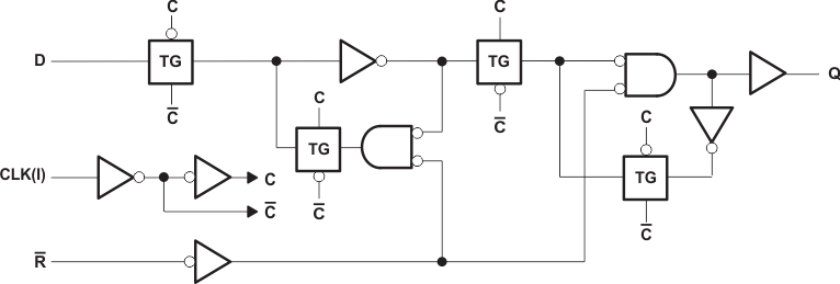
4 Simplified Schematics