SCDS167A May 2004 – July 2022 SN74CB3Q16211
PRODUCTION DATA
- 1 Features
- 2 Applications
- 3 Description
- 4 Revision History
- 5 Description (continued)
- 6 Pin Configuration and Functions
- 7 Specifications
- 8 Parameter Measurement Information
- 9 Device and Documentation Support
- 10Mechanical, Packaging, and Orderable Information
Package Options
Mechanical Data (Package|Pins)
Thermal pad, mechanical data (Package|Pins)
Orderable Information
1 Features
- Member of the Texas Instruments
Widebus® family - High-bandwidth data path (up to 500 MHz(1))
- 5-V tolerant I/Os with device powered up or powered down
- Low and flat ON-state resistance (ron)
characteristics over operating range
(ron = 5 Ω typical) - Rail-to-rail switching on data I/O ports
- 0-V to 5-V switching with 3.3-V VCC
- 0-V to 3.3-V switching with 2.5-V VCC
- Bidirectional data flow, with near-zero propagation delay
- Low input or output capacitance minimizes loading
and signal distortion
(Cio(OFF) = 4 pF typical) - Fast switching frequency (fOE = 20 MHz maximum)
- Data and control inputs provide undershoot clamp diodes
- Low power consumption (ICC = 1 mA typical)
- VCC operating range from 2.3 V to 3.6 V
- Data I/Os support 0-V to 5-V signaling levels
(0.8 V, 1.2 V, 1.5 V, 1.8 V, 2.5 V, 3.3 V, and 5 V) - Control inputs can be driven by TTL or
5-V/3.3-V CMOS outputs - Ioff supports partial-power-down mode operation
- Latch-up Performance Exceeds 100 mA Per JESD 78, Class II
- ESD Performance Tested Per JESD 22
- 2000-V Human-Body Model
(A114-B, Class II) - 1000-V Charged-Device Model (C101)
- 2000-V Human-Body Model
- Supports both digital and analog applications: PCI interface, differential signal interface, memory interleaving, bus isolation, low-distortion signal gating (1)

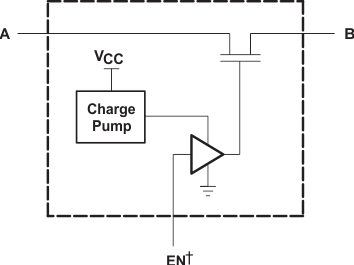
† EN is the
internal enable signal applied to the switch.
Simplified Schematic, Each FET Switch (SW)1. For additional
information regarding the performance characteristics of the CB3Q family,
refer to the TI application report, CBT-C, CB3T, and CB3Q
Signal-Switch Families.