SGLS416 January 2015 TLC2274-HT
PRODUCTION DATA.
- 1 Features
- 2 Applications
- 3 Description
- 4 Revision History
- 5 Pin Configuration and Functions
-
6 Specifications
- 6.1 Absolute Maximum Ratings
- 6.2 ESD Ratings
- 6.3 Recommended Operating Conditions
- 6.4 Thermal Information
- 6.5 Electrical Characteristics, VDD = 5 V
- 6.6 Operating Characteristics, VDD = 5 V
- 6.7 Electrical Characteristics, VDD± = ±5 V
- 6.8 Operating Characteristics, VDD± = ±5 V
- 6.9 Typical Characteristics
- 7 Detailed Description
- 8 Application and Implementation
- 9 Power Supply Recommendations
- 10Layout
- 11Device and Documentation Support
- 12Mechanical, Packaging, and Orderable Information
Package Options
Mechanical Data (Package|Pins)
- PW|14
Thermal pad, mechanical data (Package|Pins)
Orderable Information
1 Features
- Qualified for Automotive Applications
- Qualified in Accordance With AEC-Q100
- Output Swing Includes Both Supply Rails
- Low Noise: 9 nV/√Hz Typ at ƒ = 1 kHz
- Low Input Bias Current: 1 pA Typical
- Fully Specified for Both Single-Supply and Split-Supply Operation
- Common-Mode Input Voltage Range Includes Negative Rail
- High-Gain Bandwidth: 2.2 MHz Typical
- High Slew Rate: 3.6 V/μs Typical
- Low Input Offset Voltage 2500-μV Max at TA = 25°C
- Macromodel Included
2 Applications
- Supports Extreme Temperature Applications:
- Controlled Baseline
- One Assembly and Test Site
- One Fabrication Site
- Available in Extreme (–40°C to 150°C) Temperature Range (1)
- Extended Product Life Cycle
- Extended Product-Change Notification
- Product Traceability
- Texas Instruments' high temperature products use highly-optimized silicon (die) solutions with design and process enhancements to maximize performance over extended temperatures. All devices are characterized and qualified for 1000 hours continuous operating life at maximum rated temperature.
3 Description
The TLC2274 is a quadruple operational amplifier from Texas Instruments. The device exhibits rail-to-rail output performance for increased dynamic range in single- or split-supply applications. The TLC2274 offers 2 MHz of bandwidth and 3 V/μs of slew rate for higher speed applications. These device offers comparable ac performance while having better noise, input offset voltage, and power dissipation than existing CMOS operational amplifiers. The TLC2274 has a noise voltage of 9nV/√Hz, two times lower than competitive solutions.
The TLC2274, exhibiting high input impedance and low noise, is excellent for small-signal conditioning for high-impedance sources, such as piezoelectric transducers. Because of the micropower dissipation levels, this device works well in hand-held monitoring and remote-sensing applications. In addition, the rail-to-rail output feature, with single- or split-supplies, makes this device a great choice when interfacing with analog-to-digital converters (ADCs). This family is fully characterized at 5 V and ±5 V.
It offers increased output dynamic range, lower noise voltage, and lower input offset voltage. This enhanced feature set allows the device to be used in a wider range of applications.
Device Information(1)
| PART NUMBER | PACKAGE | BODY SIZE (NOM) |
|---|---|---|
| TLC2274-HT | TSSOP (14) | 6.60 mm × 5.10 mm |
- For all available packages, see the orderable addendum at the end of the data sheet.
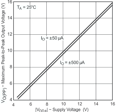
Maximum Peak-to-Peak Output Voltage
vs Supply Voltage
4 Revision History
| DATE | REVISION | NOTES |
|---|---|---|
| January 2015 | * | Initial release. |