SLOS275E January 2000 – November 2016 TPA0211
PRODUCTION DATA.
- 1 Features
- 2 Applications
- 3 Description
- 4 Revision History
- 5 Device Comparison Table
- 6 Pin Configuration and Functions
- 7 Specifications
- 8 Parameter Measurement Information
- 9 Detailed Description
- 10Application and Implementation
- 11Power Supply Recommendations
- 12Layout
- 13Device and Documentation Support
- 14Mechanical, Packaging, and Orderable Information
Package Options
Refer to the PDF data sheet for device specific package drawings
Mechanical Data (Package|Pins)
- DGN|8
Thermal pad, mechanical data (Package|Pins)
- DGN|8
Orderable Information
1 Features
- 2 W Into 4 Ω From 5-V Supply
- 0.6 W Into 4 Ω From 3-V Supply
- Wide Power Supply Compatibility: 3 V to 5 V
- Low Supply Current:
- 4 mA Typical at 5 V
- 4 mA Typical at 3 V
- Shutdown Control: 1 µA Typical
- Shutdown Pin Is TTL Compatible
- –40°C to 85°C Operating Temperature Range
- Space-Saving, Thermally-Enhanced MSOP-PowerPAD™ Packaging
2 Applications
- Wireless Communictors
- Notebook PCs
- PDAs
- Other Small Portable Audio Devices
3 Description
The TPA0211 is a 2-W mono bridge-tied-load (BTL) amplifier designed to drive speakers with as low as
4-Ω impedance. The device is ideal for small wireless communicators, notebook PCs, PDAs, anyplace a mono speaker and stereo headphones are required. From a 5-V supply, the TPA0211 can deliver 2 W of power into a 4-Ω speaker.
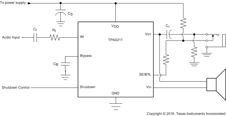
The gain of the input stage is set by the user-selected input resistor and a 50-kΩ internal feedback resistor (AV = –RF / RI). The power stage is internally configured with a gain of –1.25 V/V in SE mode, and –2.5 V/V in BTL mode. Thus, the overall gain of the amplifier is –62.5 kΩ/RI in SE mode and –125 kΩ/RI in BTL mode. The input terminals are high-impedance CMOS inputs, and can be used as summing nodes.
The TPA0211 is available in the 8-pin thermally-enhanced MSOP-PowerPAD package (DGN) and operates over an ambient temperature range of –40°C to 85°C.
Device Information(1)
| PART NUMBER | PACKAGE | BODY SIZE (NOM) |
|---|---|---|
| TPA0211 | MSOP-PowerPAD (8) | 3.00 mm × 3.00 mm |
- For all available packages, see the orderable addendum at the end of the data sheet.
Simplified Application Schematic
