SLVSBQ2D January 2013 – May 2016 TPS61163
PRODUCTION DATA.
- 1 Features
- 2 Applications
- 3 Description
- 4 Revision History
- 5 Device Comparison Table
- 6 Pin Configuration and Functions
- 7 Specifications
- 8 Detailed Description
- 9 Application and Implementation
- 10Power Supply Recommendations
- 11Layout
- 12Device and Documentation Support
- 13Mechanical, Packaging, and Orderable Information
Package Options
Mechanical Data (Package|Pins)
- YFF|9
Thermal pad, mechanical data (Package|Pins)
Orderable Information
1 Features
- 2.7-V to 6.5-V Input Voltage
- Integrated 1.5-A, 40-V MOSFET
- 1.2-MHz Switching Frequency
- Dual Current Sinks of up to 30 mA Current Each
- 1% Typical Current Matching and Accuracy
- 37.5-V Overvoltage Protection (OVP) Threshold
- Adaptive Boost Output to WLED Voltages
- Very Low Voltage Headroom Control (90 mV)
- Flexible Digital and PWM Brightness Control
- One-Wire Control Interface (EasyScale™)
- PWM Dimming Control Interface
- Up to 100:1 PWM Dimming Ratio
- Up to 10-bit Dimming Resolution
- Up to 90% Efficiency
- Overvoltage Protection
- Built-in Soft Start
- Built-in WLED Open and Short Protection
- Thermal Shutdown
- Supports 4.7-µH Inductor Application
2 Applications
3 Description
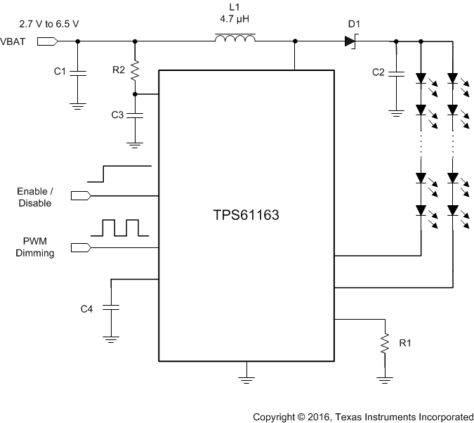
The TPS61163 is a dual-channel WLED driver that provides highly integrated solutions for single-cell Li-ion battery-powered smartphone backlights. The device has a built-in high-efficiency boost regulator with integrated 1.5-A, 40-V power MOSFET and supports a voltage as low as 2.7 V. With two high current-matching-capability current-sink regulators, the device can drive up to 10s2p WLED diodes. The boost output can automatically adjust to the WLED forward voltage and allows very low voltage-headroom control, thus effectively improving the efficiency of the LED strings.
The TPS61163 supports both a PWM dimming interface and a one-wire digital EasyScale™ dimming interface, either which can achieve 9-bit dimming control.
The TPS61163 integrates built-in soft start, overvoltage and overcurrent protection, and thermal shutdown protections.
Device Information(1)
| PART NUMBER | PACKAGE | BODY SIZE (MAX) |
|---|---|---|
| TPS61163 | DSBGA (9) | 1.336 mm × 1.336 mm |
Simplified Schematic

4 Revision History
Changes from C Revision (January 2013) to D Revision
- Added Device Information and Pin Configuration and Functions sections, ESD Ratings table, Feature Description, Device Functional Modes, Application and Implementation, Power Supply Recommendations, Layout, Device and Documentation Support, and Mechanical, Packaging, and Orderable Information sections; reformatted Thermal Information notesGo
- Changed wording of second paragraph in Boost Converter subsection Go
Changes from B Revision (March 2013) to C Revision
- Deleted TPS61162 from data sheetGo
- Changed PWM FREQ = 20kHz to PWM FREQ = 40kHz in Figure 3Go
- Changed PWM FREQ = 20kHz to PWM FREQ = 40kHz in Figure 5Go
- Changed PWM Freq = 20kHz to PWM Freq = 40kHz in the descriptions of Figure 16 - Figure 1, Figure 22, Figure 3, and Figure 5 in Go
- Changed PWM FREQ = 20kHz to PWM FREQ = 40kHz in Figure 22Go
Changes from A Revision (February 2013) to B Revision
- Initial release of the deviceGo
Changes from * Revision (January 2013) to A Revision
- Changes to the Product Preview deviceGo