SLVSA76G March 2010 – January 2016 TPS65180B , TPS65181 , TPS65181B
PRODUCTION DATA.
- 1 Features
- 2 Applications
- 3 Description
- 4 Revision History
- 5 Description (continued)
- 6 Device Comparison Table
- 7 Pin Configuration and Functions
- 8 Specifications
-
9 Detailed Description
- 9.1 Overview
- 9.2 Functional Block Diagram
- 9.3 Feature Description
- 9.4 Device Functional Modes
- 9.5
Register Maps
- 9.5.1 Thermistor Readout (TMST_VALUE) Register (Offset = 0x00h)
- 9.5.2 Enable (ENABLE) Register (Offset = 0x01h)
- 9.5.3 Positive Voltage Rail Adjustment (VP_ADJUST) Register (Offset = 0x02h)
- 9.5.4 Negative Voltage Rail Adjustment (VN_ADJUST) Register (Offset = 0x03h)
- 9.5.5 VCOM Adjustment (VCOM_ADJUST) Register (Offset = 0x04h)
- 9.5.6 Interrupt Enable 1 (INT_ENABLE1) Register (Offset = 0x05h)
- 9.5.7 Interrupt Enable 2 (INT_ENABLE2) Register (Offset = 0x06h)
- 9.5.8 Interrupt INT_STATUS1 (INT_STATUS1) Register (Offset = 0x07h)
- 9.5.9 Interrupt Status 2 (INT_STATUS2) Register (Offset = 0x08h)
- 9.5.10 Power Sequence Register 0 (PWR_SEQ0) Register (Offset = 0x09h)
- 9.5.11 Power Sequence Register 1 (PWR_SEQ1) Register (Offset = 0x0Ah)
- 9.5.12 Power Sequence Register 2 (PWR_SEQ2) Register (Offset = 0x0Bh)
- 9.5.13 Thermistor Configuration Register (TMST_CONFIG) (Offset = 0x0Ch)
- 9.5.14 Thermistor Hot Threshold (TMST_OS) Register (Offset = 0x0Dh)
- 9.5.15 Thermistor Cool Threshold (TMST_HYST) Register (Offset = 0x0Eh)
- 9.5.16 Power-Good Status (PG_STATUS) Register (Offset = 0x0Fh)
- 9.5.17 Revision and Version Control (REVID) Register (Offset = 0x10h)
- 9.5.18 I2C Read Pointer Control (FIX_READ_POINTER) Register (Offset = 0x11h) (TPS65181 and TPS65181B ONLY)
-
10Application and Implementation
- 10.1
Application Information
- 10.1.1 Dependencies Between Rails
- 10.1.2 Soft-Start
- 10.1.3 VCOM Adjustment
- 10.1.4 VCOM Adjustment Through Register Control
- 10.1.5 VCOM Adjustment Through External Potentiometer
- 10.1.6 VPOS and VNEG Supply Tracking
- 10.1.7 Fault Handling and Recovery
- 10.1.8 TPS65180 and TPS65180B Fault Handling
- 10.1.9 TPS65181 and TPS65181B Fault Handling
- 10.1.10 Power-Good Pin
- 10.1.11 Interrupt Pin
- 10.1.12 Panel Temperature Monitoring
- 10.1.13 NTC Bias Circuit
- 10.1.14 TPS65180 and TPS65180B Temperature Acquisition
- 10.1.15 TPS65181 and TPS65181B Temperature Acquisition
- 10.1.16 Overtemperature Reporting
- 10.1.17 Overtemperature Fault Queuing
- 10.1.18 TPS65181 and TPS65181B Temperature Sensor
- 10.1.19 I2C Bus Operation
- 10.2 Typical Application
- 10.1
Application Information
- 11Power Supply Recommendations
- 12Layout
- 13Device and Documentation Support
- 14Mechanical, Packaging, and Orderable Information
Package Options
Mechanical Data (Package|Pins)
- RGZ|48
Thermal pad, mechanical data (Package|Pins)
- RGZ|48
Orderable Information
1 Features
- Single-Chip Power Management Solution for
E Ink® Vizplex™ Electronic Paper Displays - Generates Positive and Negative Gate and Source Driver Voltages and Back-Plane Bias from a Single, Low-Voltage Input Supply
- 3-V to 6-V Input Voltage Range
- Boost Converter for Positive Rail Base
- Inverting Buck-Boost Converter for Negative Rail Base
- Two Adjustable LDOs for Source Driver Supply
- LDO1: 15 V, 120 mA (VPOS)
- LDO2: –15 V, 120 mA (VNEG)
- Accurate Output Voltage Tracking
- VPOS - VNEG = ±50 mV
- Two Charge Pumps for Gate Driver Supply
- CP1: 22 V, 10 mA (VDDH)
- CP2: –20 V, 12 mA, (VEE)
- Adjustable VCOM Driver for Accurate Panel-Backplane Biasing
- –0.3 V to –2.5 V
- ±1.5% Accuracy (±18 mV)
- 8-Bit Control (11-mV Nominal Step Size)
- 15-mA Maximum Integrated Switch
- Integrated 3.3-V Power Switch for Disabling System Power Rail
- Thermistor Monitoring
- –10°C to +85°C Temperature Range
- ±1°C Accuracy from 0°C to 50°C
- I2C Serial Interface
- Slave Address 0x48h (1001000)
- Flexible Power-Up Sequencing
- Interrupt and Sleep Mode Support
- Thermally-Enhanced Package for Efficient Heat Management
(48-Pin 7 mm × 7 mm × 0.9 mm VQFN)
2 Applications
- Power Supply for Active Matrix E Ink Vizplex Panels
- EPD Power Supply
- E-Book Readers
- EPSON® S1D13522 (ISIS) Timing Controller
- EPSON S1D13521 (Broadsheet) Timing Controller
- Application Processors With Integrated or Software Timing Controller (OMAP™)
3 Description
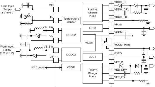
The TPS6518x and TPS65181xB family of devices are single-chip power supplies designed to for E Ink Vizplex displays used in portable e-reader applications and support panel sizes up to 9.7 inches. Two high-efficiency DC–DC boost converters generate ±17-V rails which are boosted to 22 V and –20 V by two change pumps to provide the gate driver supply for the Vizplex panel. Two tracking LDOs create the ±15-V source driver supplies which support up to 120-mA of output current. All rails are adjustable through the I2C interface to accommodate specific panel requirements.
Device Information(1)
| PART NUMBER | PACKAGE | BODY SIZE (NOM) |
|---|---|---|
| TPS65180(2) | VQFN (48) | 7.00 mm × 7.00 mm |
| TPS65180B | ||
| TPS65181(2) | ||
| TPS65181B |
- For all available packages, see the orderable addendum at the end of the data sheet.
- Not recommended for new design (NRND).
Typical Application Schematic

4 Revision History
Changes from F Revision (February 2011) to G Revision
- Added ESD Ratings table, Feature Description section, Device Functional Modes, Application and Implementation section, Power Supply Recommendations section, Layout section, Device and Documentation Support section, and Mechanical, Packaging, and Orderable Information section.Go