SLOS913A October 2015 – February 2017 SN55HVD75-EP
PRODUCTION DATA.
- 1 Features
- 2 Applications
- 3 Description
- 4 Revision History
- 5 Pin Configuration and Functions
- 6 Specifications
- 7 Parameter Measurement Information
- 8 Detailed Description
- 9 Application and Implementation
- 10Power Supply Recommendations
- 11Layout
- 12Device and Documentation Support
- 13Mechanical, Packaging, and Orderable Information
Package Options
Mechanical Data (Package|Pins)
- DRB|8
Thermal pad, mechanical data (Package|Pins)
- DRB|8
Orderable Information
7 Parameter Measurement Information
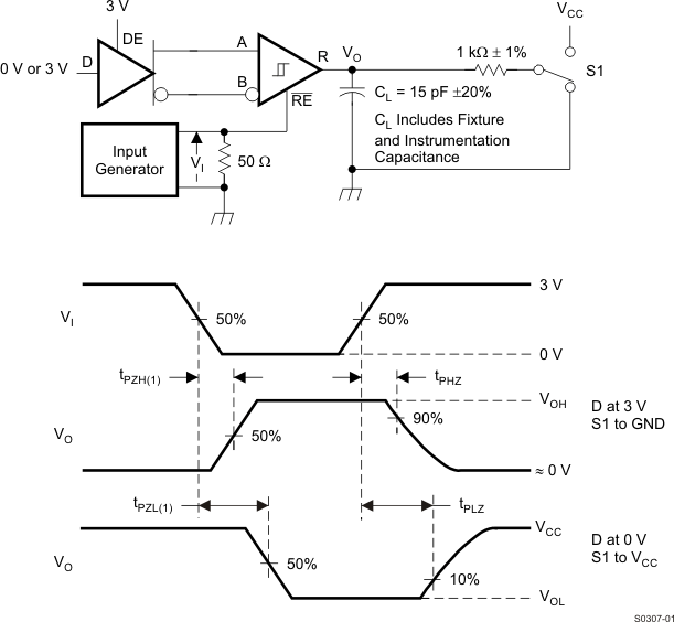
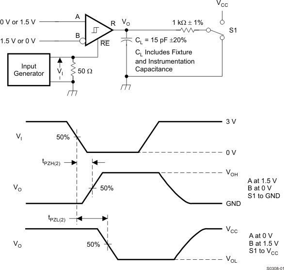
Input generator rate is 100 kbps, 50% duty cycle, rise or fall time is less than 6 ns, output impedance is 50 Ω.
 Figure 6. Measurement of Driver Differential Output Voltage With Common-Mode Load
 Figure 7. Measurement of Driver Differential and Common-Mode Output With RS-485 Load
 Figure 8. Measurement of Driver Differential Output Rise and Fall Times and Propagation Delays

D at 3 V to test non-inverting output, D at 0 V to test inverting output.
Figure 9. Measurement of Driver Enable and Disable Times With Active High Output and Pulldown Load

D at 0 V to test non-inverting output, D at 3 V to test inverting output.
Figure 10. Measurement of Driver Enable and Disable Times With Active Low Output and Pullup Load
 Figure 11. Measurement of Receiver Output Rise and Fall Times and Propagation Delays
 Figure 12. Measurement of Receiver Enable and Disable Times With Driver Enabled
 Figure 13. Measurement of Receiver Enable Times With Driver Disabled