SNAS305J July 2005 – March 2016 ADC121S021
PRODUCTION DATA.
- 1 Features
- 2 Applications
- 3 Description
- 4 Revision History
- 5 Device Comparison Table
- 6 Pin Configuration and Functions
- 7 Specifications
- 8 Parameter Measurement Information
- 9 Detailed Description
- 10Applications Information
- 11Power Supply Recommendations
- 12Layout
- 13Device and Documentation Support
- 14Mechanical, Packaging, and Orderable Information
Package Options
Mechanical Data (Package|Pins)
Thermal pad, mechanical data (Package|Pins)
Orderable Information
12 Layout
12.1 Layout Guidelines
Ground must be a low impedance connection for return currents to flow undisturbed back to their respective sources. Keep connections to the ground plane as short and direct as possible. When using vias to connect to the ground layer, use multiple vias in parallel to reduce impedance to ground.
A mixed-signal layout sometimes incorporates separate analog and digital ground planes that are tied together at one location; however, separating the ground planes is not necessary when analog, digital, and power supply circuitry into different PCB regions to prevent digital return currents from coupling into sensitive analog circuitry.
For best performance, dedicate an entire PCB layer to a ground plane and do not route any other signal traces on this layer. If ground plane separation is necessary, then make the connection at the ADC. Do not connect individual ground planes at multiple locations because this configuration creates ground loops. A single plane for analog and digital ground avoids ground loops.
If isolation is required in the application, isolate the digital signals between the ADC and controller, or provide the isolation form the controller to the remaining system. If an external crystal is used to provide the ADC clock, place the crystal and load capacitors directly to the ADC pins using short direct traces.
Supply pins must be bypassed with a low-ESR ceramic capacitor. Place the bypass capacitors as close as possible to the supply pins using short, direct traces. For optimum performance, use low-impedance connections on the ground-side connections of the bypass capacitors. Flow the supply current through the bypass capacitor pin first and then to the supply pin to make the bypassing most effective (also known as a Kelvin connection). If multiple ADCs are on the same PCB, use wide power supply traces or dedicated power-supply planes to minimize the potential of crosstalk between ADCs.
It is important that the SCLK input of the serial interface is free from noise and glitches. Even with relatively slow SCLK frequencies, short digital-signal rise and fall times may cause excessive ringing and noise. For best performance, keep the digital signal traces short, use termination resistors as needed, and ensure all digital signals are routed directly above the ground plane with minimal use of vias.
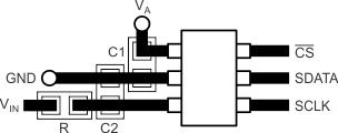
12.2 Layout Example
 Figure 22. ADC1210S21 Layout Example