SBAS670B July 2014 – April 2017 ADC3441 , ADC3442 , ADC3443 , ADC3444
PRODUCTION DATA.
- 1 Features
- 2 Applications
- 3 Description
- 4 Revision History
- 5 Device Comparison Table
- 6 Pin Configuration and Functions
-
7 Specifications
- 7.1 Absolute Maximum Ratings
- 7.2 ESD Ratings
- 7.3 Recommended Operating Conditions
- 7.4 Thermal Information
- 7.5 Electrical Characteristics: General
- 7.6 Electrical Characteristics: ADC3441, ADC3442
- 7.7 Electrical Characteristics: ADC3443, ADC3444
- 7.8 AC Performance: ADC3441
- 7.9 AC Performance: ADC3442
- 7.10 AC Performance: ADC3443
- 7.11 AC Performance: ADC3444
- 7.12 Digital Characteristics
- 7.13 Timing Requirements: General
- 7.14 Timing Requirements: LVDS Output
- 7.15 Typical Characteristics: ADC3441
- 7.16 Typical Characteristics: ADC3442
- 7.17 Typical Characteristics: ADC3443
- 7.18 Typical Characteristics: ADC3444
- 7.19 Typical Characteristics: Common
- 7.20 Typical Characteristics: Contour
- 8 Parameter Measurement Information
-
9 Detailed Description
- 9.1 Overview
- 9.2 Functional Block Diagram
- 9.3 Feature Description
- 9.4 Device Functional Modes
- 9.5 Programming
- 9.6
Register Maps
- 9.6.1
Serial Register Description
- 9.6.1.1 Register 01h (address = 01h)
- 9.6.1.2 Register 03h (address = 03h)
- 9.6.1.3 Register 04h (address = 04h)
- 9.6.1.4 Register 05h (address = 05h)
- 9.6.1.5 Register 06h (address = 06h)
- 9.6.1.6 Register 07h (address = 07h)
- 9.6.1.7 Register 09h (address = 09h)
- 9.6.1.8 Register 0Ah (address = 0Ah)
- 9.6.1.9 Register 0Bh (address = 0Bh)
- 9.6.1.10 Register 13h (address = 13h)
- 9.6.1.11 Register 0Eh (address = 0Eh)
- 9.6.1.12 Register 0Fh (address = 0Fh)
- 9.6.1.13 Register 15h (address = 15h)
- 9.6.1.14 Register 25h (address = 25h)
- 9.6.1.15 Register 27h (address = 27h)
- 9.6.1.16 Register 11Dh (address = 11Dh)
- 9.6.1.17 Register 122h (address = 122h)
- 9.6.1.18 Register 134h (address = 134h)
- 9.6.1.19 Register 139h (address = 139h)
- 9.6.1.20 Register 21Dh (address = 21Dh)
- 9.6.1.21 Register 222h (address = 222h)
- 9.6.1.22 Register 234h (address = 234h)
- 9.6.1.23 Register 239h (address = 239h)
- 9.6.1.24 Register 308h (address = 308h)
- 9.6.1.25 Register 41Dh (address = 41Dh)
- 9.6.1.26 Register 422h (address = 422h)
- 9.6.1.27 Register 434h (address = 434h)
- 9.6.1.28 Register 439h (address = 439h)
- 9.6.1.29 Register 51Dh (address = 51Dh)
- 9.6.1.30 Register 522h (address = 522h)
- 9.6.1.31 Register 534h (address = 534h)
- 9.6.1.32 Register 539h (address = 539h)
- 9.6.1.33 Register 608h (address = 608h)
- 9.6.1.34 Register 70Ah (address = 70Ah)
- 9.6.1
Serial Register Description
- 10Applications and Implementation
- 11Power Supply Recommendations
- 12Layout
- 13Device and Documentation Support
- 14Mechanical, Packaging, and Orderable Information
Package Options
Mechanical Data (Package|Pins)
- RTQ|56
Thermal pad, mechanical data (Package|Pins)
- RTQ|56
Orderable Information
7 Specifications
7.1 Absolute Maximum Ratings
over operating free-air temperature range (unless otherwise noted)(1)| MIN | MAX | UNIT | ||
|---|---|---|---|---|
| Analog supply voltage range, AVDD | –0.3 | 2.1 | V | |
| Digital supply voltage range, DVDD | –0.3 | 2.1 | V | |
| Voltage applied to input pins |
INAP, INBP, INAM, INBM | –0.3 | min (1.9, AVDD + 0.3) | V |
| CLKP, CLKM | –0.3 | AVDD + 0.3 | ||
| SYSREFP, SYSREFM | –0.3 | AVDD + 0.3 | ||
| SCLK, SEN, SDATA, RESET, PDN | –0.3 | 3.9 | ||
| Temperature | Operating free-air, TA | –40 | 85 | ºC |
| Operating junction, TJ | 125 | |||
| Storage, Tstg | –65 | 150 | ||
(1) Stresses beyond those listed under Absolute Maximum Ratings may cause permanent damage to the device. These are stress ratings only, which do not imply functional operation of the device at these or any other conditions beyond those indicated under Recommended Operating Conditions. Exposure to absolute-maximum-rated conditions for extended periods may affect device reliability.
7.2 ESD Ratings
| VALUE | UNIT | |||
|---|---|---|---|---|
| V(ESD) | Electrostatic discharge | Human body model (HBM), per ANSI/ESDA/JEDEC JS-001(1) | ±2000 | V |
(1) JEDEC document JEP155 states that 500-V HBM allows safe manufacturing with a standard ESD control process.
7.3 Recommended Operating Conditions
over operating free-air temperature range (unless otherwise noted)(3)| MIN | NOM | MAX | UNIT | |||
|---|---|---|---|---|---|---|
| SUPPLIES | ||||||
| AVDD | Analog supply voltage range | 1.7 | 1.8 | 1.9 | V | |
| DVDD | Digital supply voltage range | 1.7 | 1.8 | 1.9 | V | |
| ANALOG INPUT | ||||||
| VID | Differential input voltage | For input frequencies < 450 MHz | 2 | VPP | ||
| For input frequencies < 600 MHz | 1 | |||||
| VIC | Input common-mode voltage | VCM ± 0.025 | V | |||
| CLOCK INPUT | ||||||
| Input clock frequency | Sampling clock frequency | 15(2) | 125(1) | MSPS | ||
| Input clock amplitude (differential) | Sine wave, ac-coupled | 0.2 | 1.5 | VPP | ||
| LPECL, ac-coupled | 1.6 | |||||
| LVDS, ac-coupled | 0.7 | |||||
| Input clock duty cycle | 35% | 50% | 65% | |||
| Input clock common-mode voltage | 0.95 | V | ||||
| DIGITAL OUTPUTS | ||||||
| CLOAD | External load capacitance from each output pin to GND | 3.3 | pF | |||
| RLOAD | Differential load resistance to be placed across the positive and negative pins of the LVDS output pair | 100 | Ω | |||
(1) With the clock divider enabled by default for divide-by-1. Maximum sampling clock frequency for the divide-by-4 option is 500 MSPS.
(2) See Table 3 for details.
(3) After power-up, only use the RESET pin to reset the device for the first time; see the Register Initialization section for details.
7.4 Thermal Information
| THERMAL METRIC(1) | ADC344x | UNIT | |
|---|---|---|---|
| RTQ (VQFN) | |||
| 56 PINS | |||
| RθJA | Junction-to-ambient thermal resistance | 25.3 | °C/W |
| RθJC(top) | Junction-to-case (top) thermal resistance | 9.5 | °C/W |
| RθJB | Junction-to-board thermal resistance | 3.4 | °C/W |
| ψJT | Junction-to-top characterization parameter | 0.2 | °C/W |
| ψJB | Junction-to-board characterization parameter | 3.3 | °C/W |
| RθJC(bot) | Junction-to-case (bottom) thermal resistance | 0.5 | °C/W |
(1) For more information about traditional and new thermal metrics, see the Semiconductor and IC Package Thermal Metrics application report.
7.5 Electrical Characteristics: General
at maximum sampling rate, 50% clock duty cycle, AVDD = DVDD = 1.8 V, and –1-dBFS differential input (unless otherwise noted); typical values are specified at an ambient temperature of 25°C; minimum and maximum values are specified over an ambient temperature range of –40°C to +85°C| PARAMETER | TEST CONDITIONS | MIN | TYP | MAX | UNIT | ||
|---|---|---|---|---|---|---|---|
| ANALOG INPUT | |||||||
| Differential input full-scale | 2.0 | VPP | |||||
| ri | Input resistance | Differential at dc | 6.6 | kΩ | |||
| ci | Input capacitance | Differential at dc | 3.7 | pF | |||
| VOC(VCM) | VCM common-mode voltage output | 0.8 | 0.95 | 1.1 | V | ||
| VCM output current capability | 10 | mA | |||||
| Input common-mode current | Per analog input pin | 1.5 | µA/MSPS | ||||
| Analog input bandwidth (–3-dB point) |
50-Ω differential source driving 50-Ω termination across INP and INM | 540 | MHz | ||||
| DC ACCURACY | |||||||
| EO | Offset error | –25 | 25 | mV | |||
| αEO | Temperature coefficient of offset error | ±0.024 | mV/°C | ||||
| EG | Overall dc gain error of a channel | ADC3441 | –2 | 2 | %FS | ||
| ADC3442, ADC3443, ADC3444 | -2.5 | 2.5 | |||||
| αEG | Temperature coefficient of overall gain error | 0.005 | Δ%FS/°C | ||||
| CHANNEL-TO-CHANNEL ISOLATION | |||||||
| Crosstalk(1)(2) | fIN = 10 MHz | Between near channels | 105 | dB | |||
| Between far channels | 105 | ||||||
| fIN = 100 MHz | Between near channels | 95 | |||||
| Between far channels | 105 | ||||||
| fIN = 200 MHz | Between near channels | 94 | |||||
| Between far channels | 105 | ||||||
| fIN = 230 MHz | Between near channels | 92 | |||||
| Between far channels | 105 | ||||||
| fIN = 300 MHz | Between near channels | 85 | |||||
| Between far channels | 105 | ||||||
(1) Crosstalk is measured with a –1-dBFS input signal on the aggressor channel and no input on the victim channel.
(2) Channels A and B are near to each other but far from channels C and D. Similarly, channels C and D are near to each other but far from channels A and B; see the Pin Configuration and Functions section for more information.
7.6 Electrical Characteristics: ADC3441, ADC3442
at maximum sampling rate, 50% clock duty cycle, AVDD = DVDD = 1.8 V, and –1-dBFS differential input (unless otherwise noted); typical values are specified at an ambient temperature of 25°C; minimum and maximum values are specified over an ambient temperature range of –40°C to +85°C| PARAMETER | ADC3441 | ADC3442 | UNIT | |||||
|---|---|---|---|---|---|---|---|---|
| MIN | TYP | MAX | MIN | TYP | MAX | |||
| ADC clock frequency | 25 | 50 | MSPS | |||||
| Resolution | 14 | 14 | Bits | |||||
| 1.8-V analog supply current | 54 | 74 | 71 | 97 | mA | |||
| 1.8-V digital supply current | 45 | 67 | 56 | 83 | mA | |||
| Total power dissipation | 177 | 215 | 228 | 277 | mW | |||
| Global power-down dissipation | 5 | 17 | 5 | 17 | mW | |||
| Standby power-down dissipation | 34 | 103 | 35 | 103 | mW | |||
7.7 Electrical Characteristics: ADC3443, ADC3444
at maximum sampling rate, 50% clock duty cycle, AVDD = DVDD = 1.8 V, and –1-dBFS differential input (unless otherwise noted); typical values are specified at an ambient temperature of 25°C; minimum and maximum values are specified over an ambient temperature range of –40°C to +85°C| PARAMETER | ADC3443 | ADC3444 | UNIT | |||||
|---|---|---|---|---|---|---|---|---|
| MIN | TYP | MAX | MIN | TYP | MAX | |||
| ADC clock frequency | 80 | 125 | MSPS | |||||
| Resolution | 14 | 14 | Bits | |||||
| 1.8-V analog supply current | 92 | 125 | 119 | 162 | mA | |||
| 1.8-V digital supply current | 68 | 101 | 98 | 145 | mA | |||
| Total power dissipation | 288 | 350 | 391 | 475 | mW | |||
| Global power-down dissipation | 5 | 17 | 5 | 17 | mW | |||
| Standby power-down dissipation | 40 | 103 | 43 | 103 | mW | |||
7.8 AC Performance: ADC3441
at maximum sampling rate, 50% clock duty cycle, AVDD = DVDD = 1.8 V, and –1-dBFS differential input (unless otherwise noted); typical values are specified at an ambient temperature of 25°C; minimum and maximum values are specified over an ambient temperature range of –40°C to +85°C| PARAMETER | TEST CONDITIONS | ADC3441 (fS = 25 MSPS) | UNIT | ||||||
|---|---|---|---|---|---|---|---|---|---|
| DITHER ON | DITHER OFF | ||||||||
| MIN | TYP | MAX | MIN | TYP | MAX | ||||
| SNR | Signal-to-noise ratio (from 1-MHz offset) |
fIN = 10 MHz | 73.1 | 73.5 | dBFS | ||||
| fIN = 20 MHz | 70.9 | 72.9 | 73.4 | ||||||
| fIN = 70 MHz | 72.5 | 73 | |||||||
| fIN = 100 MHz | 72.4 | 72.7 | |||||||
| fIN = 170 MHz | 71.4 | 71.7 | |||||||
| fIN = 230 MHz | 70.3 | 70.5 | |||||||
| Signal-to-noise ratio (full Nyquist band) |
fIN = 10 MHz | 72.4 | 72.9 | ||||||
| fIN = 20 MHz | 72.2 | 72.7 | |||||||
| fIN = 70 MHz | 71.9 | 72.4 | |||||||
| fIN = 100 MHz | 71.7 | 72.0 | |||||||
| fIN = 170 MHz | 70.9 | 71.1 | |||||||
| fIN = 230 MHz | 69.7 | 69.9 | |||||||
| NSD(1) | Noise spectral density (averaged across Nyquist zone) | fIN = 10 MHz | –143.7 | –144.1 | dBFS/Hz | ||||
| fIN = 20 MHz | –143.5 | –141.5 | –143.9 | ||||||
| fIN = 70 MHz | –143.1 | –143.6 | |||||||
| fIN = 100 MHz | –143.0 | –143.3 | |||||||
| fIN = 170 MHz | –142.0 | –142.3 | |||||||
| fIN = 230 MHz | –140.9 | –141.1 | |||||||
| SINAD(1) | Signal-to-noise and distortion ratio | fIN = 10 MHz | 73.1 | 73.4 | dBFS | ||||
| fIN = 20 MHz | 69.9 | 72.9 | 73.2 | ||||||
| fIN = 70 MHz | 71.7 | 71.9 | |||||||
| fIN = 100 MHz | 72.6 | 72.8 | |||||||
| fIN = 170 MHz | 71.2 | 71.4 | |||||||
| fIN = 230 MHz | 69.9 | 70.1 | |||||||
| ENOB(1) | Effective number of bits | fIN = 10 MHz | 11.9 | 11.9 | Bits | ||||
| fIN = 20 MHz | 11.3 | 11.8 | 11.8 | ||||||
| fIN = 70 MHz | 11.7 | 11.8 | |||||||
| fIN = 100 MHz | 11.8 | 11.8 | |||||||
| fIN = 170 MHz | 11.5 | 11.6 | |||||||
| fIN = 230 MHz | 11.3 | 11.4 | |||||||
| SFDR | Spurious-free dynamic range | fIN = 10 MHz | 91 | 89 | dBc | ||||
| fIN = 20 MHz | 82 | 91 | 85 | ||||||
| fIN = 70 MHz | 92 | 87 | |||||||
| fIN = 100 MHz | 85 | 82 | |||||||
| fIN = 170 MHz | 86 | 85 | |||||||
| fIN = 230 MHz | 81 | 81 | |||||||
| HD2 | Second-order harmonic distortion | fIN = 10 MHz | 92 | 93 | dBc | ||||
| fIN = 20 MHz | 82 | 92 | 91 | ||||||
| fIN = 70 MHz | 92 | 91 | |||||||
| fIN = 100 MHz | 96 | 94 | |||||||
| fIN = 170 MHz | 86 | 85 | |||||||
| fIN = 230 MHz | 84 | 84 | |||||||
| HD3 | Third-order harmonic distortion | fIN = 10 MHz | 96 | 90 | dBc | ||||
| fIN = 20 MHz | 82 | 93 | 89 | ||||||
| fIN = 70 MHz | 93 | 88 | |||||||
| fIN = 100 MHz | 85 | 82 | |||||||
| fIN = 170 MHz | 89 | 89 | |||||||
| fIN = 230 MHz | 82 | 82 | |||||||
| Non HD2, HD3 |
Spurious-free dynamic range (excluding HD2, HD3) | fIN = 10 MHz | 100 | 93 | dBc | ||||
| fIN = 20 MHz | 87 | 97 | 92 | ||||||
| fIN = 70 MHz | 97 | 92 | |||||||
| fIN = 100 MHz | 97 | 94 | |||||||
| fIN = 170 MHz | 92 | 90 | |||||||
| fIN = 230 MHz | 98 | 92 | |||||||
| THD | Total harmonic distortion | fIN = 10 MHz | 90 | 86 | dBc | ||||
| fIN = 20 MHz | 79 | 90 | 85 | ||||||
| fIN = 70 MHz | 90 | 85 | |||||||
| fIN = 100 MHz | 84 | 80 | |||||||
| fIN = 170 MHz | 84 | 83 | |||||||
| fIN = 230 MHz | 80 | 80 | |||||||
| IMD3 | Two-tone, third-order intermodulation distortion | fIN1 = 45 MHz, fIN2 = 50 MHz, each tone at –7 dBFS |
–97 | –97 | dBFS | ||||
| fIN1 = 185 MHz, fIN2 = 190 MHz, each tone at –7 dBFS |
–88 | –88 | |||||||
| INL | Integral nonlinearity | fIN = 20 MHz | ±0.75 | ±3 | ±0.75 | LSBs | |||
| DNL | Differential nonlinearity | fIN = 20 MHz | –0.95 | ±0.6 | ±0.6 | LSBs | |||
(1) Reported from a 1-MHz offset.
7.9 AC Performance: ADC3442
at maximum sampling rate, 50% clock duty cycle, AVDD = DVDD = 1.8 V, and –1-dBFS differential input (unless otherwise noted); typical values are specified at an ambient temperature of 25°C; minimum and maximum values are specified over an ambient temperature range of –40°C to +85°C| PARAMETER | TEST CONDITIONS | ADC3442 (fS = 50 MSPS) | UNIT | ||||||
|---|---|---|---|---|---|---|---|---|---|
| DITHER ON | DITHER OFF | ||||||||
| MIN | TYP | MAX | MIN | TYP | MAX | ||||
| SNR | Signal-to-noise ratio (from 1-MHz offset) |
fIN = 10 MHz | 73.1 | 73.5 | dBFS | ||||
| fIN = 20 MHz | 70.7 | 72.9 | 73.3 | ||||||
| fIN = 70 MHz | 72.7 | 73.1 | |||||||
| fIN = 100 MHz | 71.9 | 72.6 | |||||||
| fIN = 170 MHz | 71.5 | 71.8 | |||||||
| fIN = 230 MHz | 70.4 | 70.8 | |||||||
| Signal-to-noise ratio (full Nyquist band) |
fIN = 10 MHz | 72.5 | 72.9 | ||||||
| fIN = 20 MHz | 72.3 | 72.7 | |||||||
| fIN = 70 MHz | 71.9 | 72.3 | |||||||
| fIN = 100 MHz | 71.3 | 72.1 | |||||||
| fIN = 170 MHz | 71.0 | 71.2 | |||||||
| fIN = 230 MHz | 69.8 | 70.2 | |||||||
| NSD(1) | Noise spectral density (averaged across Nyquist zone) | fIN = 10 MHz | –146.9 | –147.3 | dBFS/Hz | ||||
| fIN = 20 MHz | –146.7 | –144.5 | –146.9 | ||||||
| fIN = 70 MHz | –146.5 | –146.9 | |||||||
| fIN = 100 MHz | –145.7 | –146.4 | |||||||
| fIN = 170 MHz | –145.3 | –145.6 | |||||||
| fIN = 230 MHz | –144.2 | –144.6 | |||||||
| SINAD(1) | Signal-to-noise and distortion ratio | fIN = 10 MHz | 73 | 73.4 | dBFS | ||||
| fIN = 20 MHz | 69.7 | 72.2 | 72.7 | ||||||
| fIN = 70 MHz | 72.2 | 72.7 | |||||||
| fIN = 100 MHz | 72.1 | 73.2 | |||||||
| fIN = 170 MHz | 71.4 | 71.8 | |||||||
| fIN = 230 MHz | 69.8 | 70.1 | |||||||
| ENOB(1) | Effective number of bits | fIN = 10 MHz | 11.9 | 11.9 | Bits | ||||
| fIN = 20 MHz | 11.3 | 11.8 | 11.8 | ||||||
| fIN = 70 MHz | 11.8 | 11.8 | |||||||
| fIN = 100 MHz | 11.7 | 11.9 | |||||||
| fIN = 170 MHz | 11.6 | 11.6 | |||||||
| fIN = 230 MHz | 11.4 | 11.4 | |||||||
| SFDR | Spurious-free dynamic range | fIN = 10 MHz | 90 | 90 | dBc | ||||
| fIN = 20 MHz | 82 | 92 | 90 | ||||||
| fIN = 70 MHz | 92 | 90 | |||||||
| fIN = 100 MHz | 87 | 87 | |||||||
| fIN = 170 MHz | 86 | 84 | |||||||
| fIN = 230 MHz | 83 | 82 | |||||||
| HD2 | Second-order harmonic distortion | fIN = 10 MHz | 95 | 92 | dBc | ||||
| fIN = 20 MHz | 83 | 99 | 94 | ||||||
| fIN = 70 MHz | 93 | 91 | |||||||
| fIN = 100 MHz | 92 | 92 | |||||||
| fIN = 170 MHz | 87 | 85 | |||||||
| fIN = 230 MHz | 85 | 83 | |||||||
| HD3 | Third-order harmonic distortion | fIN = 10 MHz | 90 | 92 | dBc | ||||
| fIN = 20 MHz | 82 | 94 | 91 | ||||||
| fIN = 70 MHz | 94 | 91 | |||||||
| fIN = 100 MHz | 87 | 87 | |||||||
| fIN = 170 MHz | 88 | 89 | |||||||
| fIN = 230 MHz | 83 | 88 | |||||||
| Non HD2, HD3 |
Spurious-free dynamic range (excluding HD2, HD3) | fIN = 10 MHz | 99 | 95 | dBc | ||||
| fIN = 20 MHz | 87 | 99 | 93 | ||||||
| fIN = 70 MHz | 99 | 93 | |||||||
| fIN = 100 MHz | 92 | 94 | |||||||
| fIN = 170 MHz | 97 | 89 | |||||||
| fIN = 230 MHz | 97 | 91 | |||||||
| THD | Total harmonic distortion | fIN = 10 MHz | 89 | 87 | dBc | ||||
| fIN = 20 MHz | 79 | 90 | 87 | ||||||
| fIN = 70 MHz | 90 | 87 | |||||||
| fIN = 100 MHz | 86 | 85 | |||||||
| fIN = 170 MHz | 85 | 83 | |||||||
| fIN = 230 MHz | 81 | 81 | |||||||
| IMD3 | Two-tone, third-order intermodulation distortion | fIN1 = 45 MHz, fIN2 = 50 MHz |
–92 | –92 | dBFS | ||||
| fIN1 = 185 MHz, fIN2 = 190 MHz |
–87 | –87 | |||||||
| INL | Integral nonlinearity | fIN = 20 MHz | ±0.8 | ±3 | ±0.8 | LSBs | |||
| DNL | Differential nonlinearity | fIN = 20 MHz | –0.95 | ±0.6 | ±0.6 | LSBs | |||
(1) Reported from a 1-MHz offset.
7.10 AC Performance: ADC3443
at maximum sampling rate, 50% clock duty cycle, AVDD = DVDD = 1.8 V, and –1-dBFS differential input (unless otherwise noted); typical values are specified at an ambient temperature of 25°C; minimum and maximum values are specified over an ambient temperature range of –40°C to +85°C| PARAMETER | TEST CONDITIONS | ADC3443 (fS = 80 MSPS) | UNIT | ||||||
|---|---|---|---|---|---|---|---|---|---|
| DITHER ON | DITHER OFF | ||||||||
| MIN | TYP | MAX | MIN | TYP | MAX | ||||
| SNR | Signal-to-noise ratio (from 1-MHz offset) |
fIN = 10 MHz | 72.9 | 73.2 | dBFS | ||||
| fIN = 70 MHz | 70.7 | 72.8 | 73.1 | ||||||
| fIN = 100 MHz | 72.5 | 72.9 | |||||||
| fIN = 170 MHz | 72.1 | 72.4 | |||||||
| fIN = 230 MHz | 71.4 | 71.7 | |||||||
| Signal-to-noise ratio (full Nyquist band) |
fIN = 10 MHz | 72.5 | 72.8 | ||||||
| fIN = 70 MHz | 72.4 | 72.8 | |||||||
| fIN = 100 MHz | 72.1 | 72.6 | |||||||
| fIN = 170 MHz | 71.7 | 72.0 | |||||||
| fIN = 230 MHz | 71.1 | 71.4 | |||||||
| NSD(1) | Noise spectral density (averaged across Nyquist zone) | fIN = 10 MHz | –148.8 | –149.1 | dBFS/Hz | ||||
| fIN = 70 MHz | –148.7 | –146.6 | –149.0 | ||||||
| fIN = 100 MHz | –148.4 | –148.8 | |||||||
| fIN = 170 MHz | –148.0 | –148.3 | |||||||
| fIN = 230 MHz | –147.3 | –147.6 | |||||||
| SINAD(1) | Signal-to-noise and distortion ratio | fIN = 10 MHz | 72.8 | 73.2 | dBFS | ||||
| fIN = 70 MHz | 69.7 | 72.2 | 72.4 | ||||||
| fIN = 100 MHz | 72.7 | 73 | |||||||
| fIN = 170 MHz | 71.9 | 72.2 | |||||||
| fIN = 230 MHz | 71.2 | 71.4 | |||||||
| ENOB(1) | Effective number of bits | fIN = 10 MHz | 11.8 | 11.9 | Bits | ||||
| fIN = 70 MHz | 11.3 | 11.8 | 11.8 | ||||||
| fIN = 100 MHz | 11.8 | 11.8 | |||||||
| fIN = 170 MHz | 11.7 | 11.7 | |||||||
| fIN = 230 MHz | 11.5 | 11.6 | |||||||
| SFDR | Spurious-free dynamic range | fIN = 10 MHz | 89 | 89 | dBc | ||||
| fIN = 70 MHz | 81 | 90 | 89 | ||||||
| fIN = 100 MHz | 92 | 92 | |||||||
| fIN = 170 MHz | 88 | 86 | |||||||
| fIN = 230 MHz | 86 | 84 | |||||||
| HD2 | Second-order harmonic distortion | fIN = 10 MHz | 94 | 91 | dBc | ||||
| fIN = 70 MHz | 81 | 96 | 91 | ||||||
| fIN = 100 MHz | 97 | 94 | |||||||
| fIN = 170 MHz | 88 | 86 | |||||||
| fIN = 230 MHz | 87 | 85 | |||||||
| HD3 | Third-order harmonic distortion | fIN = 10 MHz | 89 | 90 | dBc | ||||
| fIN = 70 MHz | 81 | 91 | 90 | ||||||
| fIN = 100 MHz | 94 | 100 | |||||||
| fIN = 170 MHz | 95 | 93 | |||||||
| fIN = 230 MHz | 87 | 87 | |||||||
| Non HD2, HD3 |
Spurious-free dynamic range (excluding HD2, HD3) | fIN = 10 MHz | 100 | 95 | dBc | ||||
| fIN = 70 MHz | 86 | 98 | 94 | ||||||
| fIN = 100 MHz | 95 | 94 | |||||||
| fIN = 170 MHz | 95 | 94 | |||||||
| fIN = 230 MHz | 94 | 92 | |||||||
| THD | Total harmonic distortion | fIN = 10 MHz | 88 | 86 | dBc | ||||
| fIN = 70 MHz | 78 | 89 | 87 | ||||||
| fIN = 100 MHz | 91 | 90 | |||||||
| fIN = 170 MHz | 87 | 84 | |||||||
| fIN = 230 MHz | 84 | 82 | |||||||
| IMD3 | Two-tone, third-order intermodulation distortion | fIN1 = 45 MHz, fIN2 = 50 MHz |
–98 | –98 | dBFS | ||||
| fIN1 = 185 MHz, fIN2 = 190 MHz |
–88 | –88 | |||||||
| INL | Integral nonlinearity | fIN = 70 MHz | ±0.8 | ±3 | ±0.8 | LSBs | |||
| DNL | Differential nonlinearity | fIN = 70 MHz | –0.95 | ±0.7 | ±0.7 | LSBs | |||
(1) Reported from a 1-MHz offset.
7.11 AC Performance: ADC3444
at maximum sampling rate, 50% clock duty cycle, AVDD = DVDD = 1.8 V, and –1-dBFS differential input (unless otherwise noted); typical values are specified at an ambient temperature of 25°C; minimum and maximum values are specified over an ambient temperature range of –40°C to +85°C| PARAMETER | TEST CONDITIONS | ADC3444 (fS = 125 MSPS) | UNIT | ||||||
|---|---|---|---|---|---|---|---|---|---|
| DITHER ON | DITHER OFF | ||||||||
| MIN | TYP | MAX | MIN | TYP | MAX | ||||
| SNR | Signal-to-noise ratio (from 1-MHz offset) |
fIN = 10 MHz | 72.6 | 73 | dBFS | ||||
| fIN = 70 MHz | 70.2 | 72.5 | 72.9 | ||||||
| fIN = 100 MHz | 72.2 | 72.7 | |||||||
| fIN = 170 MHz | 71.7 | 72.3 | |||||||
| fIN = 230 MHz | 70.8 | 71.7 | |||||||
| Signal-to-noise ratio (full Nyquist band) |
fIN = 10 MHz | 72.4 | 72.8 | ||||||
| fIN = 70 MHz | 72.3 | 72.7 | |||||||
| fIN = 100 MHz | 72.1 | 72.5 | |||||||
| fIN = 170 MHz | 71.5 | 72.1 | |||||||
| fIN = 230 MHz | 70.6 | 71.5 | |||||||
| NSD(1) | Noise spectral density (averaged across Nyquist zone) | fIN = 10 MHz | –150.4 | –150.9 | dBFS/Hz | ||||
| fIN = 70 MHz | –150.4 | –148.1 | –150.8 | ||||||
| fIN = 100 MHz | –150.1 | –150.5 | |||||||
| fIN = 170 MHz | –149.5 | –150.2 | |||||||
| fIN = 230 MHz | –148.7 | –149.6 | |||||||
| SINAD(1) | Signal-to-noise and distortion ratio | fIN = 10 MHz | 72.6 | 72.9 | dBFS | ||||
| fIN = 70 MHz | 69.3 | 72.3 | 72.7 | ||||||
| fIN = 100 MHz | 72.3 | 72.7 | |||||||
| fIN = 170 MHz | 71.5 | 72 | |||||||
| fIN = 230 MHz | 69.9 | 70.6 | |||||||
| ENOB(1) | Effective number of bits | fIN = 10 MHz | 11.8 | 11.8 | Bits | ||||
| fIN = 70 MHz | 11.2 | 11.8 | 11.8 | ||||||
| fIN = 100 MHz | 11.7 | 11.8 | |||||||
| fIN = 170 MHz | 11.6 | 11.7 | |||||||
| fIN = 230 MHz | 11.4 | 11.6 | |||||||
| SFDR | Spurious-free dynamic range | fIN = 10 MHz | 92 | 87 | dBc | ||||
| fIN = 70 MHz | 80 | 93 | 88 | ||||||
| fIN = 100 MHz | 89 | 89 | |||||||
| fIN = 170 MHz | 86 | 84 | |||||||
| fIN = 230 MHz | 82 | 82 | |||||||
| HD2 | Second-order harmonic distortion | fIN = 10 MHz | 93 | 93 | dBc | ||||
| fIN = 70 MHz | 80 | 94 | 91 | ||||||
| fIN = 100 MHz | 90 | 90 | |||||||
| fIN = 170 MHz | 86 | 85 | |||||||
| fIN = 230 MHz | 81 | 80 | |||||||
| HD3 | Third-order harmonic distortion | fIN = 10 MHz | 96 | 88 | dBc | ||||
| fIN = 70 MHz | 81 | 95 | 89 | ||||||
| fIN = 100 MHz | 95 | 89 | |||||||
| fIN = 170 MHz | 93 | 87 | |||||||
| fIN = 230 MHz | 87 | 86 | |||||||
| Non HD2, HD3 |
Spurious-free dynamic range (excluding HD2, HD3) | fIN = 10 MHz | 100 | 93 | dBc | ||||
| fIN = 70 MHz | 86 | 99 | 94 | ||||||
| fIN = 100 MHz | 94 | 92 | |||||||
| fIN = 170 MHz | 96 | 93 | |||||||
| fIN = 230 MHz | 94 | 90 | |||||||
| THD | Total harmonic distortion | fIN = 10 MHz | 91 | 85 | dBc | ||||
| fIN = 70 MHz | 77 | 91 | 85 | ||||||
| fIN = 100 MHz | 88 | 86 | |||||||
| fIN = 170 MHz | 85 | 82 | |||||||
| fIN = 230 MHz | 80 | 78 | |||||||
| IMD3 | Two-tone, third-order intermodulation distortion | fIN1 = 45 MHz, fIN2 = 50 MHz |
–97 | –97 | dBFS | ||||
| fIN1 = 185 MHz, fIN2 = 190 MHz |
–87 | –87 | |||||||
| INL | Integral nonlinearity | fIN = 70 MHz | ±0.75 | ±3 | ±0.75 | LSBs | |||
| DNL | Differential nonlinearity | fIN = 70 MHz | –0.95 | ±0.7 | ±0.7 | LSBs | |||
(1) Reported from a 1-MHz offset.
7.12 Digital Characteristics
the dc specifications refer to the condition where the digital outputs are not switching, but are permanently at a valid logic level 0 or 1; AVDD = DVDD = 1.8 V, and –1-dBFS differential input (unless otherwise noted)| PARAMETER | TEST CONDITIONS | MIN | TYP | MAX | UNIT | ||
|---|---|---|---|---|---|---|---|
| DIGITAL INPUTS (RESET, SCLK, SDATA, SEN, PDN) | |||||||
| VIH | High-level input voltage | All digital inputs support 1.8-V and 3.3-V CMOS logic levels | 1.3 | V | |||
| VIL | Low-level input voltage | 0.4 | V | ||||
| IIH | High-level input current | RESET, SDATA, SCLK, PDN | VHIGH = 1.8 V | 10 | µA | ||
| SEN(1) | VHIGH = 1.8 V | 0 | |||||
| IIL | Low-level input current | RESET, SDATA, SCLK, PDN | VLOW = 0 V | 0 | µA | ||
| SEN | VLOW = 0 V | 10 | |||||
| DIGITAL INPUTS (SYSREFP, SYSREFM) | |||||||
| Differential swing | 0.2 | 0.8 | 1.0 | V | |||
| Common-mode voltage for SYSREF(2) | 0.9 | V | |||||
| DIGITAL OUTPUTS (CMOS Interface, SDOUT) | |||||||
| VOH | High-level output voltage | DVDD – 0.1 | DVDD | V | |||
| VOL | Low-level output voltage | 0 | 0.1 | V | |||
| DIGITAL OUTPUTS (LVDS Interface) | |||||||
| VODH | High-level output differential voltage | With an external 100-Ω termination | 280 | 350 | –280 | mV | |
| VODL | Low-level output differential voltage | With an external 100-Ω termination | –460 | –350 | –460 | mV | |
| VOCM | Output common-mode voltage | 0.9 | 1.05 | 1.2 | V | ||
(1) SEN has an internal 150-kΩ pullup resistor to AVDD. SPI pins (SEN, SCLK, SDATA) may be driven by 1.8 V or 3.3 V CMOS buffers.
(2) SYSREF is internally biased to 0.9 V.
7.13 Timing Requirements: General
typical values are at TA = 25°C, AVDD = DVDD = 1.8 V, and –1-dBFS differential input (unless otherwise noted); minimum and maximum values are across the full temperature range: TMIN = –40°C to TMAX = +85°C| MIN | TYP | MAX | UNIT | |||
|---|---|---|---|---|---|---|
| tA | Aperture delay | 1.24 | 1.44 | 1.64 | ns | |
| Aperture delay matching between two channels of the same device | ±70 | ps | ||||
| Variation of aperture delay between two devices at the same temperature and supply voltage | ±150 | ps | ||||
| tJ | Aperture jitter | 130 | fS rms | |||
| Wake-up time | Time to valid data after exiting standby power-down mode | 35 | 200 | µs | ||
| Time to valid data after exiting global power-down mode (in this mode, both channels power down) | 85 | 450 | µs | |||
| ADC latency(6) | 2-wire mode (default) | 9 | Clock cycles | |||
| 1-wire mode | 8 | Clock cycles | ||||
| tSU_SYSREF | SYSREF reference time | Setup time for SYSREF referenced to input clock falling edge | 1000 | ps | ||
| tH_SYSREF | Hold time for SYSREF referenced to input clock falling edge | 100 | ps | |||
7.14 Timing Requirements: LVDS Output
typical values are at 25°C, AVDD = DVDD = 1.8 V, –1-dBFS differential input, 7x serialization (2-wire mode), CLOAD = 3.3 pF(2), and RLOAD = 100 Ω(3) (unless otherwise noted); minimum and maximum values are across the full temperature range: TMIN = –40°C to TMAX = +85°C(4)(1)| MIN | TYP | MAX | UNIT | ||||
|---|---|---|---|---|---|---|---|
| tSU | Data setup time: data valid to zero-crossing of differential output clock (CLKOUTP – CLKOUTM)(5) |
0.36 | 0.42 | ns | |||
| tHO | Data hold time: zero-crossing of differential output clock (CLKOUTP – CLKOUTM) to data becoming invalid(5) | 0.36 | 0.47 | ns | |||
| LVDS bit clock duty cycle: duty cycle of differential clock (CLKOUTP – CLKOUTM) | 49% | ||||||
| tPDI | Clock propagation delay: input clock falling edge cross-over to frame clock rising edge cross-over 15 MSPS < sampling frequency < 125 MSPS |
1-wire mode | 2.7 | 4.5 | 6.5 | ns | |
| 2-wire mode | 0.44 × tS + tDELAY | ns | |||||
| tDELAY | Delay time | 3 | 4.5 | 5.9 | ns | ||
| tFALL, tRISE |
Data fall time, data rise time: rise time measured from –100 mV to 100 mV, 15 MSPS ≤ Sampling frequency ≤ 125 MSPS |
0.11 | ns | ||||
| tCLKRISE, tCLKFALL |
Output clock rise time, output clock fall time: rise time measured from –100 mV to 100 mV, 15 MSPS ≤ Sampling frequency ≤ 125 MSPS |
0.11 | ns | ||||
(1) Timing parameters are ensured by design and characterization and are not tested in production.
(2) CLOAD is the effective external single-ended load capacitance between each output pin and ground
(3) RLOAD is the differential load resistance between the LVDS output pair.
(4) Measurements are done with a transmission line of a 100-Ω characteristic impedance between the device and load. Setup and hold time specifications take into account the effect of jitter on the output data and clock.
(5) Data valid refers to a logic high of +100 mV and a logic low of –100 mV.
(6) Overall latency = ADC latency + tPDI; see Figure 141.
Table 1. LVDS Timings at Lower Sampling Frequencies: 7x Serialization (2-Wire Mode)
| SAMPLING FREQUENCY (MSPS) | SETUP TIME (tSU, ns) |
HOLD TIME (tHO, ns) |
||||
|---|---|---|---|---|---|---|
| MIN | TYP | MAX | MIN | TYP | MAX | |
| 25 | 2.27 | 2.6 | 2.41 | 2.6 | ||
| 40 | 1.44 | 1.6 | 1.51 | 1.7 | ||
| 50 | 1.2 | 1.32 | 1.24 | 1.4 | ||
| 60 | 0.95 | 1.04 | 0.97 | 1.09 | ||
| 80 | 0.68 | 0.75 | 0.72 | 0.81 | ||
| 100 | 0.5 | 0.57 | 0.53 | 0.62 | ||
Table 2. LVDS Timings at Lower Sampling Frequencies: 14x Serialization (1-Wire Mode)
| SAMPLING FREQUENCY (MSPS) | SETUP TIME (tSU, ns) |
HOLD TIME (tHO, ns) |
||||
|---|---|---|---|---|---|---|
| MIN | TYP | MAX | MIN | TYP | MAX | |
| 25 | 1.1 | 1.24 | 1.19 | 1.34 | ||
| 40 | 0.66 | 0.72 | 0.74 | 0.82 | ||
| 50 | 0.48 | 0.55 | 0.54 | 0.64 | ||
| 60 | 0.35 | 0.41 | 0.42 | 0.51 | ||
| 80 | 0.17 | 0.24 | 0.3 | 0.38 | ||
7.15 Typical Characteristics: ADC3441
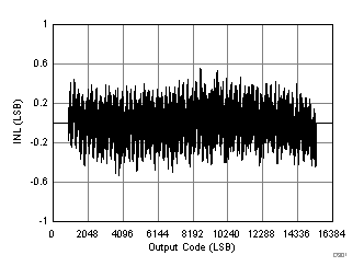
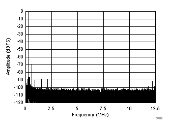
typical values are at TA = 25°C, ADC sampling rate = 25 MSPS, 50% clock duty cycle, AVDD = 1.8 V, DVDD = 1.8 V, –1-dBFS differential input, 2-VPP full-scale, 32k-point FFT, chopper disabled, SNR reported with a 1-MHz offset from dc when chopper is disabled and from fS / 2 when chopper is enabled, and dither on (unless otherwise noted)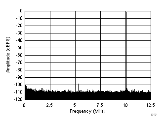
| SFDR = 98 dBc, SNR = 73.1 dBFS, SINAD = 73 dBFS, THD = 97 dBc, HD2 = 110.0 dBc, HD3 = 98 dBc, SFDR = 100 dBc (excluding HD2, HD3) |

| SFDR = 92 dBc, SNR = 72.5 dBFS, SINAD = 72.3 dBFS, THD = 91 dBc, HD2 = 108 dBc, HD3 = 92 dBc, SFDR = 101 dBc (excluding HD2, HD3) |
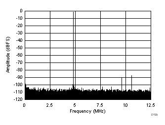
| SFDR = 87 dBc, SNR = 71.5 dBFS, SINAD = 71.1 dBFS, THD = 85 dBc, HD2 = 90 dBc, HD3 = 87 dBc, SFDR = 100 dBc (excluding HD2, HD3) |
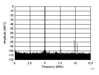
| SFDR = 76 dBc, SNR = 69.4 dBFS, SINAD = 68.8 dBFS, THD = 75 dBc, HD2 = 76 dBc, HD3 = 83 dBc, SFDR = 96 dBc (excluding HD2, HD3) |
| SFDR = 68 dBc, SNR = 66.7 dBFS, SINAD = 66.5 dBFS, THD = 92 dBc, HD2 = 68 dBc, HD3 = 90 dBc, SFDR = 91 dBc (excluding HD2, HD3) |
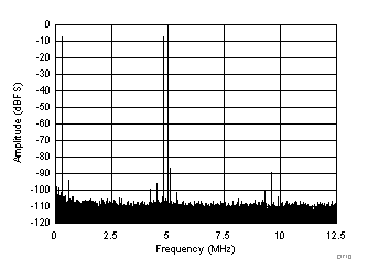
| fIN1 = 46.3 MHz, fIN2 = 50.3 MHz, IMD3 = 86 dBFS, each tone at –7 dBFS |
(–7 dBFS at 46 MHz and 50 MHz)
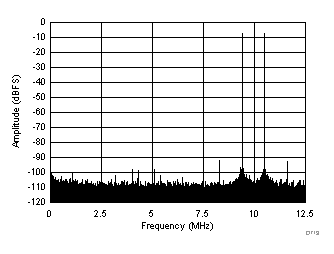
| fIN1 = 184.5 MHz, fIN2 = 189.5 MHz, IMD3 = 93 dBFS, each tone at –7 dBFS |
(–7 dBFS at 185 MHz and 190 MHz)
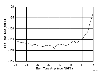
(46 MHz and 50 MHz)
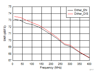
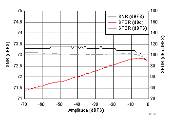
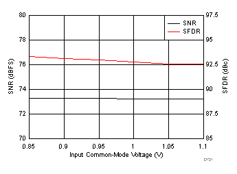
(30 MHz)
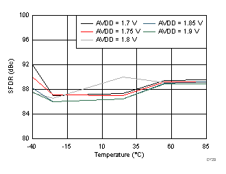
AVDD Supply and Temperature (30 MHz)
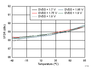
DVDD Supply and Temperature (30 MHz)

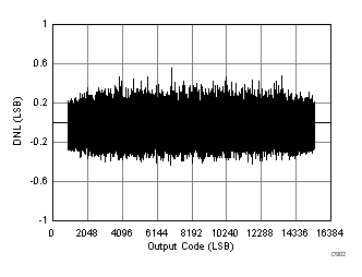
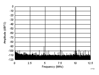
| RMS Noise = 1.33 LSBs |
| SFDR = 90 dBc, SNR = 73.5 dBFS, SINAD = 73.2 dBFS, THD = 88 dBc, HD2 = 90 dBc, HD3 = 100 dBc, SFDR = 92 dBc (excluding HD2, HD3) |

| SFDR = 90 dBc, SNR = 72.9 dBFS, SINAD = 72.7 dBFS, THD = 89 dBc, HD2 = 90 dBc, HD3 = 101 dBc, SFDR = 93 dBc (excluding HD2, HD3) |
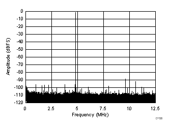
| SFDR = 88 dBc, SNR = 71.7 dBFS, SINAD = 71.4 dBFS, THD = 85 dBc, HD2 = 88 dBc, HD3 = 91 dBc, SFDR = 93 dBc (excluding HD2, HD3) |
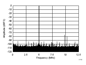
| SFDR = 75 dBc, SNR = 69.6 dBFS, SINAD = 68.6 dBFS, THD = 74 dBc, HD2 = 75 dBc, HD3 = 80 dBc, SFDR = 91 dBc (excluding HD2, HD3) |
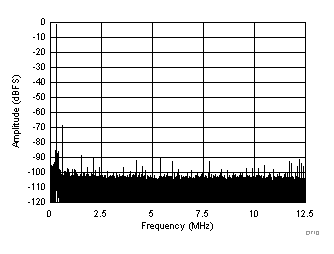
| SFDR = 66 dBc, SNR = 66.8 dBFS, SINAD = 66.5 dBFS, THD = 88 dBc, HD2 = 66 dBc, HD3 = 97 dBc, SFDR = 90 dBc (excluding HD2, HD3) |
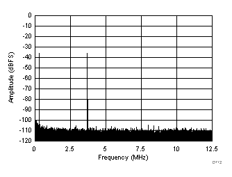
| fIN1 = 46.3 MHz, fIN2 = 50.3 MHz, IMD3 = 105 dBFS, each tone at –36 dBFS |
(–36 dBFS at 46 MHz and 50 MHz)
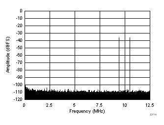
| fIN1 = 184.5 MHz, fIN2 = 189.5 MHz, IMD3 = 109 dBFS, each tone at –36 dBFS |
(–36 dBFS at 185 MHz and 190 MHz)
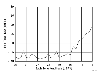
(185 MHz and 190 MHz)
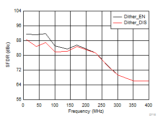
Input Frequency

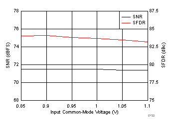
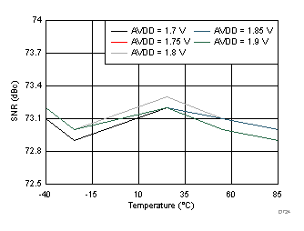
AVDD Supply and Temperature (30 MHz)
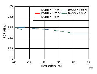
DVDD Supply and Temperature (30 MHz)
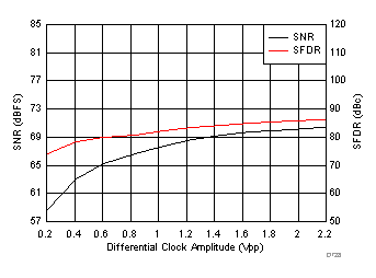
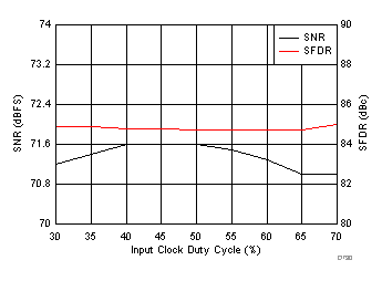
7.16 Typical Characteristics: ADC3442
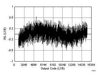
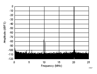
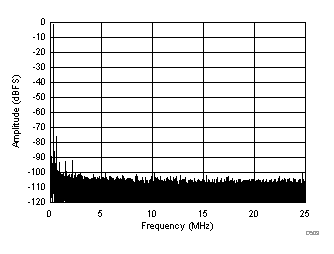
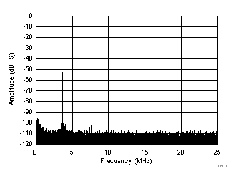
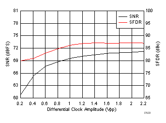
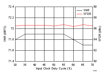
typical values are at TA = 25°C, ADC sampling rate = 50 MSPS, 50% clock duty cycle, AVDD = 1.8 V, DVDD = 1.8 V, –1-dBFS differential input, 2-VPP full-scale, 32k-point FFT, chopper disabled, SNR reported with a 1-MHz offset from dc when chopper is disabled and from fS / 2 when chopper is enabled, and dither on (unless otherwise noted)
(Chopper On, Dither On)

| SFDR = 86 dBc, SNR = 72.7 dBFS, SINAD = 72.5 dBFS, THD = 85 dBc, HD2 = 92 dBc, HD3 = 86 dBc, SFDR = 100 dBc (excluding HD2, HD3) |
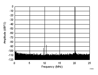
| SFDR = 86 dBc, SNR = 71.6 dBFS, SINAD = 71.4 dBFS, THD = 85 dBc, HD2 = 92 dBc, HD3 = 86 dBc, SFDR = 99 dBc (excluding HD2, HD3) |
| SFDR = 75 dBc, SNR = 70.3 dBFS, SINAD = 69.1 dBFS, THD = 74 dBc, HD2 = -75 dBc, HD3 = 81 dBc, SFDR = 95 dBc (excluding HD2, HD3) |
| SFDR = 68 dBc, SNR = 68.2 dBFS, SINAD = 68 dBFS, THD = 86 dBc, HD2 = 68 dBc, HD3 = 87 dBc |
| fIN1 = 46.3 MHz, fIN2 = 50.3 MHz, IMD3 = 102 dBFS, each tone at –7 dBFS |
(–7 dBFS at 46 MHz and 50 MHz)
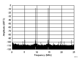
| fIN1 = 185 MHz, fIN2 = 190 MHz, IMD3 = 93 dBFS, each tone at –7 dBFS |
(–7 dBFS at 185 MHz and 190 MHz)
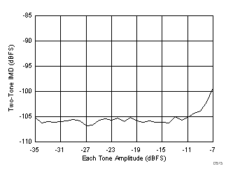
(46 MHz and 50 MHz)
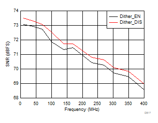
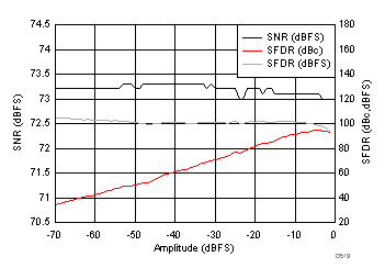

(30 MHz)
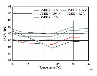
AVDD Supply and Temperature (30 MHz)
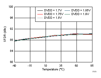
DVDD Supply and Temperature (30 MHz)


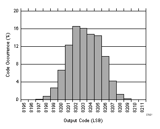
| RMS noise = 1.3 LSBs |
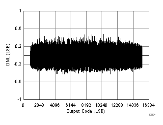
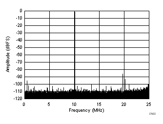
| SFDR = 85 dBc, SNR = 73.5 dBFS, SINAD = 73.3 dBFS, THD = 84 dBc, HD2 = 92 dBc, HD3 = 85 dBc, SFDR = 96 dBc (excluding HD2, HD3) |
(Chopper On, Dither Off)

| SFDR = 90 dBc, SNR = 73.1 dBFS, SINAD = 73 dBFS, THD = 88 dBc, HD2 = 92 dBc, HD3 = 90 dBc, SFDR = 95 dBc (excluding HD2, HD3) |
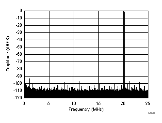
| SFDR = 90 dBc, SNR = 71.8 dBFS, SINAD = 71.6 dBFS, THD = 87 dBc, HD2 = 90 dBc, HD3 = 108 dBc, SFDR = 93 dBc (excluding HD2, HD3) |
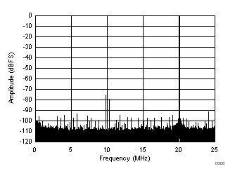
| SFDR = 75 dBc, SNR = 70.6 dBFS, SINAD = 69.6 dBFS, THD = 73 dBc, HD2 = 75 dBc, HD3 = 78 dBc, SFDR = 91 dBc (excluding HD2, HD3) |
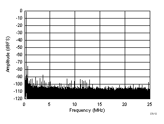
| SFDR = 68 dBc, SNR = 68.5 dBFS, SINAD = 68.3 dBFS, THD = 86 dBc, HD2 = 68 dBc, HD3 = 90 dBc |

| fIN1 = 46.3 MHz, fIN2 = 50.3 MHz, IMD3 = 110 dBFS, each tone at –36 dBFS |
(–36 dBFS at 46 MHz and 50 MHz)

| fIN1 = 185 MHz, fIN2 = 190 MHz, IMD3 = 105 dBFS, each tone at –36 dBFS |
(–36 dBFS at 185 MHz and 190 MHz)
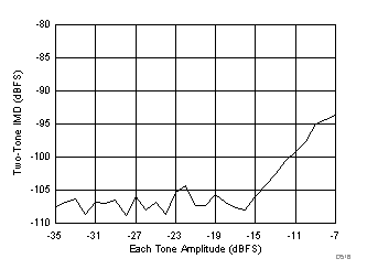
(185 MHz and 190 MHz)

Input Frequency
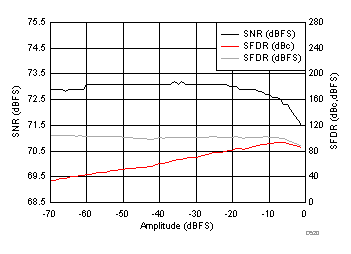
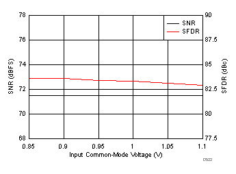

AVDD Supply and Temperature (30 MHz)
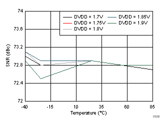
DVDD Supply and Temperature (30 MHz)
7.17 Typical Characteristics: ADC3443
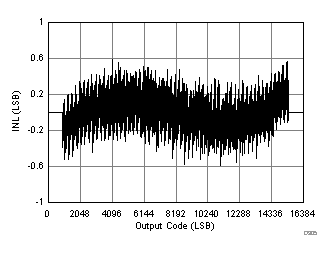
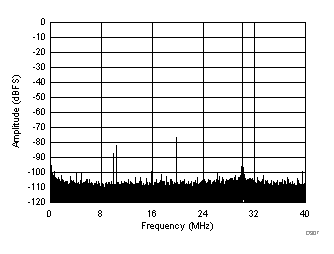
typical values are at TA = 25°C, ADC sampling rate = 80 MSPS, 50% clock duty cycle, AVDD = 1.8 V, DVDD = 1.8 V, –1-dBFS differential input, 2-VPP full-scale, 32k-point FFT, chopper disabled, SNR reported with a 1-MHz offset from dc when chopper is disabled and from fS / 2 when chopper is enabled, and dither on (unless otherwise noted)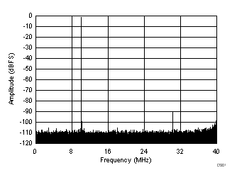 Figure 67. FFT for 10-MHz Input Signal
 (Chopper On, Dither On)
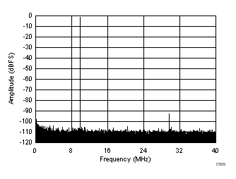
| SFDR = 91 dBc, SNR = 72.9 dBFS, SINAD = 72.8 dBFS, THD = 91 dBc, HD2 = 110 dBc, HD3 = 91 dBc |

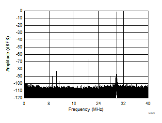
| SFDR = 95 dBc, SNR = 72.1 dBFS, SINAD = 71.9 dBFS, THD = 93 dBc, HD2 = 106 dBc, HD3 = 95 dBc |
| SFDR = 75 dBc, SNR = 70.5 dBFS, SINAD = 69.6 dBFS, THD = 74 dBc, HD2 = 75 dBc, HD3 = 81 dBc |
| SFDR = 66 dBc, SNR = 68.4 dBFS, SINAD = 64.6 dBFS, THD = 66 dBc, HD2 = 66 dBc, HD3 = 89 dBc |
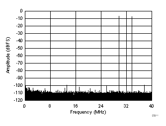
| fIN1 = 46 MHz, fIN2 = 50 MHz, IMD3 = 99 dBFS, each tone at –7 dBFS |
(–7 dBFS at 46 MHz and 50 MHz)
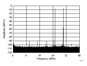
| fIN1 = 185 MHz, fIN2 = 190 MHz, IMD3 = 90 dBFS, each tone at –7 dBFS |
(–7 dBFS at 185 MHz and 190 MHz)
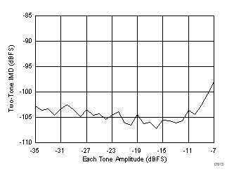
(46 MHz and 50 MHz)
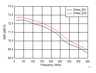
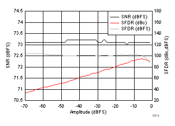
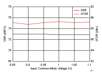
(30 MHz)
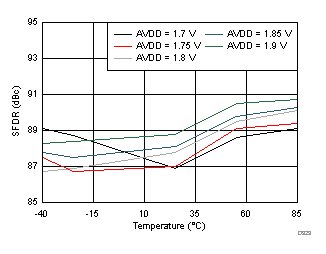
AVDD Supply and Temperature (170 MHz)
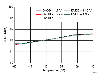
DVDD Supply and Temperature (170 MHz)
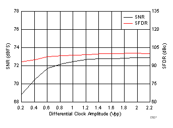
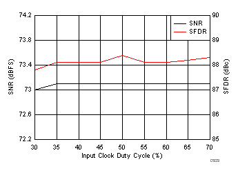
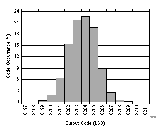
| RMS noise = 1.28 LSBs |

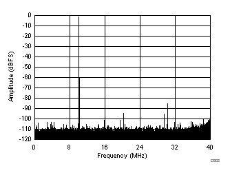
| SFDR = 84 dBc, SNR = 73.2 dBFS, SINAD = 73.1 dBFS, THD = 83 dBc, HD2 = 94 dBc, HD3 = 84 dBc |
(Chopper On, Dither Off)
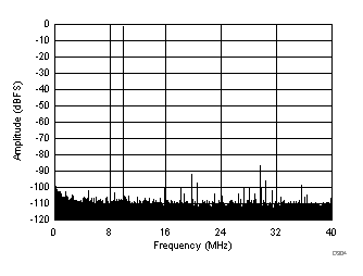
| SFDR = 85 dBc, SNR = 73.1 dBFS, SINAD = 72.9 dBFS, THD = 84 dBc, HD2 = 91 dBc, HD3 = 85 dBc |
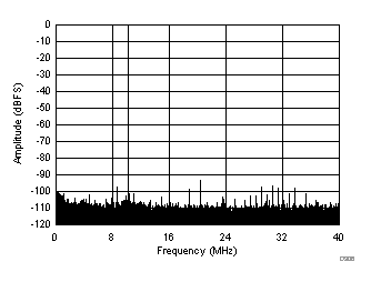
| SFDR = 92 dBc, SNR = 72.4 dBFS, SINAD = 72.2 dBFS, THD = 88 dBc, HD2 = 92 dBc, HD3 = 95 dBc |
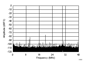
| SFDR = 75 dBc, SNR = 71 dBFS, SINAD = 69.7 dBFS, THD = 74 dBc, HD2 = 75 dBc, HD3 = 81 dBc |
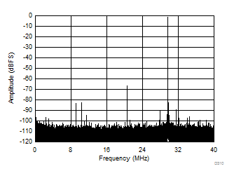
| SFDR = 65 dBc, SNR = 68.7 dBFS, SINAD = 64.4 dBFS, THD = 65 dBc, HD2 = 65 dBc, HD3 = 82 dBc |
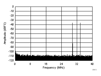
| fIN1 = 46 MHz, fIN2 = 50 MHz, IMD3 = 105 dBFS, each tone at –36 dBFS |
(–36 dBFS at 46 MHz and 50 MHz)
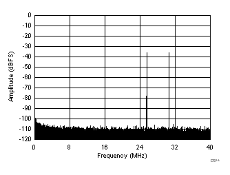
| fIN1 = 185 MHz, fIN2 = 190 MHz, IMD3 = 106 dBFS, each tone at –36 dBFS |
(–36 dBFS at 185 MHz and 190 MHz)
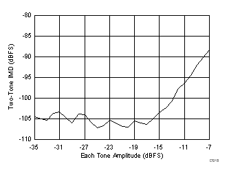
(185 MHz and 190 MHz)
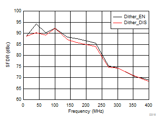
Input Frequency
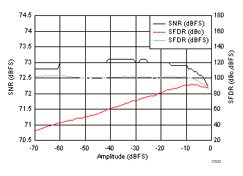
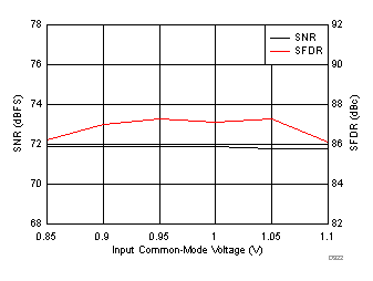
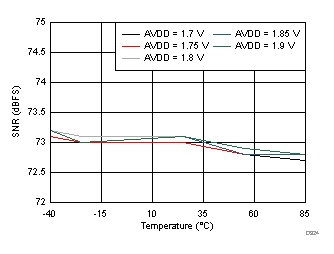
AVDD Supply and Temperature (170 MHz)
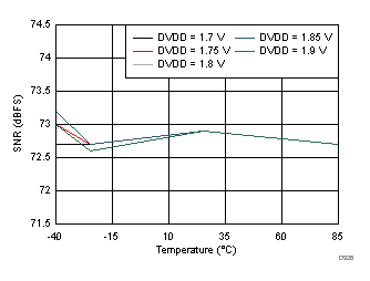
DVDD Supply and Temperature (170 MHz)
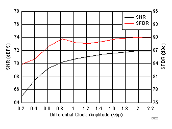
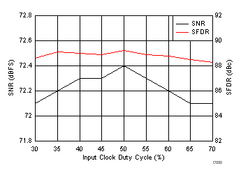
7.18 Typical Characteristics: ADC3444
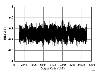
typical values are at TA = 25°C, ADC sampling rate = 125 MSPS, 50% clock duty cycle, AVDD = 1.8 V, DVDD = 1.8 V, –1-dBFS differential input, 2-VPP full-scale, 32k-point FFT, chopper disabled, SNR reported with a 1-MHz offset from dc when chopper is disabled and from fS / 2 when chopper is enabled, and dither on (unless otherwise noted)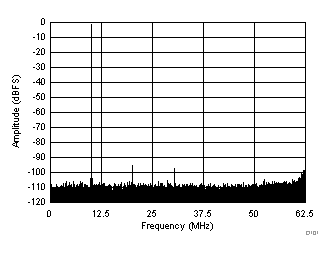 Figure 100. FFT for 10-MHz Input Signal
 (Chopper On, Dither On)
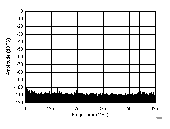
| SFDR = 96 dBc, SNR = 72.5 dBFS, SINAD = 72.4 dBFS, THD = 94 dBc, HD2 = 101 dBc, HD3 = 96 dBc |

| SFDR = 86 dBc, SNR = 71.7 dBFS, SINAD = 71.6 dBFS, THD = 93 dBc, HD2 = 86 dBc, HD3 = 99 dBc |
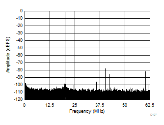
| SFDR = 77 dBc, SNR = 70.4 dBFS, SINAD = 69.6 dBFS, THD = 75 dBc, HD2 = 77 dBc, HD3 = 81 dBc |
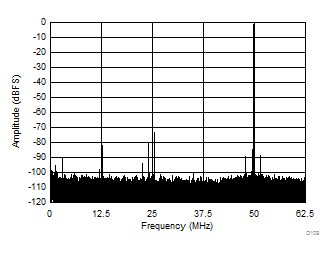
| SFDR = 72 dBc, SNR = 68.2 dBFS, SINAD = 67.3 dBFS, THD = 74 dBc, HD2 = 72 dBc, HD3 = 79 dBc |
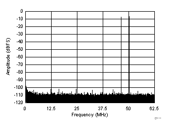
| fIN1 = 46 MHz, fIN2 = 50 MHz, IMD3 = 102 dBFS, each tone at –7 dBFS |
(–7 dBFS at 46 MHz and 50 MHz)
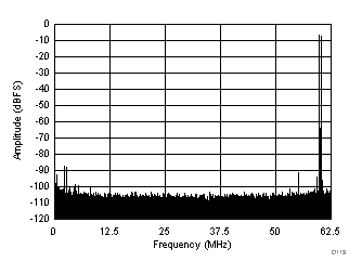
| fIN1 = 185 MHz, fIN2 = 190 MHz, IMD3 = 88 dBFS, each tone at –7 dBFS |
(–7 dBFS at 185 MHz and 190 MHz)
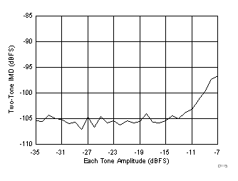
(46 MHz and 50 MHz)
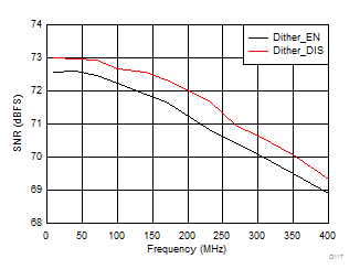

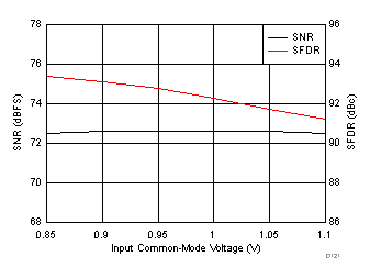
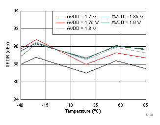
AVDD Supply and Temperature (170 MHz)
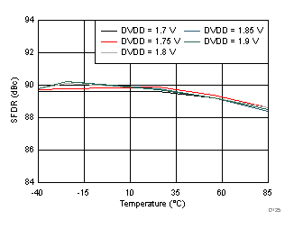
DVDD Supply and Temperature (170 MHz)
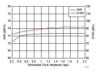
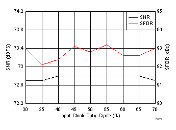

| RMS noise = 1.4 LSBs |

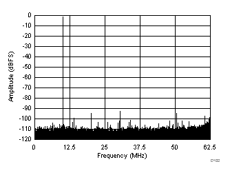
| SFDR = 91.8 dBc, SNR = 73.1 dBFS, SINAD = 73 dBFS, THD = 87 dBc, HD2 = 94 dBc, HD3 = 92 dBc |
(Chopper On, Dither Off)

| SFDR = 91 dBc, SNR = 73 dBFS, SINAD = 72.8 dBFS, THD = 87 dBc, HD2 = 91 dBc, HD3 = 95 dBc |
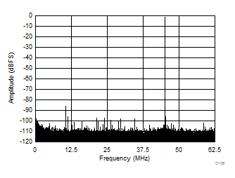
| SFDR = 85 dBc, SNR = 72.3 dBFS, SINAD = 72.1 dBFS, THD = 87 dBc, HD2 = 97 dBc, HD3 = 85 dBc |
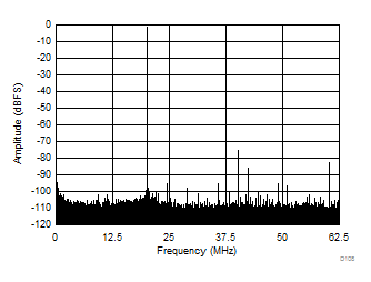
| SFDR = 74 dBc, SNR = 71 dBFS, SINAD = 70.1 dBFS, THD = 75 dBc, HD2 = 76 dBc, HD3 = 82 dBc |
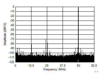
| SFDR = 70 dBc, SNR = 68.9 dBFS, SINAD = 67.6 dBFS, THD = 73 dBc, HD2 = 77 dBc, HD3 = 70 dBc |
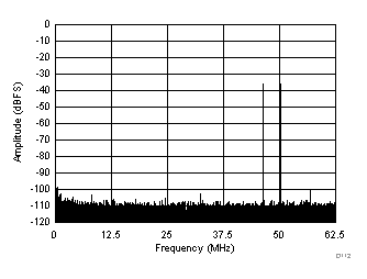
| fIN1 = 46 MHz, fIN2 = 50 MHz, IMD3 = 100 dBFS, each tone at –36 dBFS |
(–36 dBFS at 46 MHz and 50 MHz)
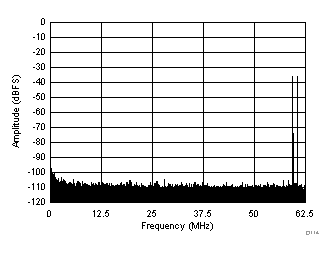
| fIN1 = 185 MHz, fIN2 = 190 MHz, IMD3 = 104 dBFS, each tone at –36 dBFS |
(–36 dBFS at 185 MHz and 190 MHz)
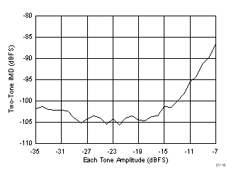
(185 MHz and 190 MHz)
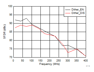
Input Frequency

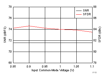
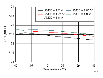
AVDD Supply and Temperature (170 MHz)
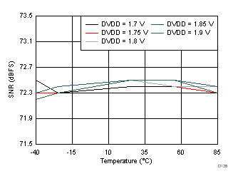
DVDD Supply and Temperature (170 MHz)
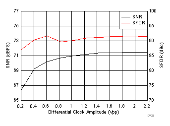
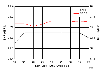
7.19 Typical Characteristics: Common
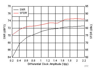
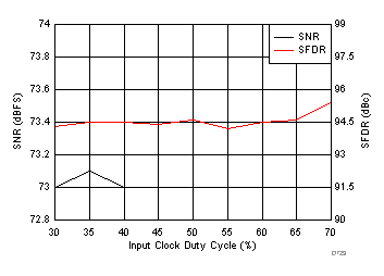
typical values are at TA = 25°C, ADC sampling rate = 125 MSPS, 50% clock duty cycle, AVDD = 1.8 V, DVDD = 1.8 V, –1-dBFS differential input, 2-VPP full-scale, 32k-point FFT, chopper disabled, SNR reported with a 1-MHz offset from dc when chopper is disabled and from fS / 2 when chopper is enabled, and dither on (unless otherwise noted)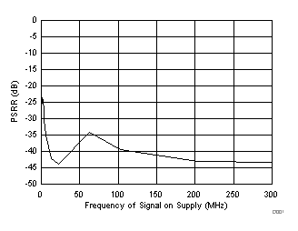
| fIN = 30 MHz, AIN = –1 dBFS, test signal amplitude = 50 mVPP |
Test Signal Frequency
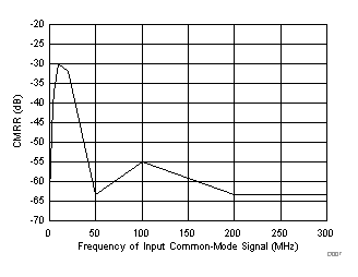
| fIN = 170 MHz, AIN = –1 dBFS, test signal amplitude = 50 mVPP, input VCM = 0.95 V |
Test Signal Frequency
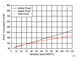
(Two-Wire Mode)
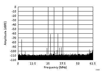 Figure 134. Power-Supply Rejection Ratio Spectrum (Chopper On)
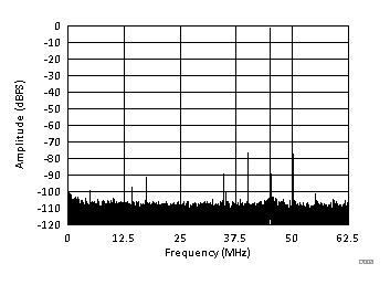
| fIN = 170.1 MHz, fCMRR = 5 MHz, ACMRR = 50 mVPP, SINAD = 69.66 dBFS, SFDR = 75.66 dBc |
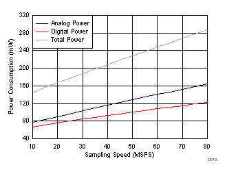
(One-Wire Mode)
7.20 Typical Characteristics: Contour
typical values are at TA = 25°C, ADC sampling rate = 125 MSPS, 50% clock duty cycle, AVDD = 1.8 V, DVDD = 1.8 V, –1-dBFS differential input, 2-VPP full-scale, 32k-point FFT, chopper disabled, SNR reported with a 1-MHz offset from dc when chopper is disabled and from fS / 2 when is chopper enabled, and dither on (unless otherwise noted)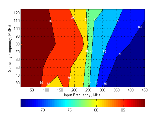 Figure 139. Spurious-Free Dynamic Range (SFDR)
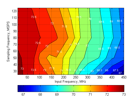 Figure 140. Signal-to-Noise Ratio (SNR)
