SBAS991B February   2021  – September 2022 ADC3661 , ADC3662 , ADC3663

PRODUCTION DATA  

  1. Features
  2. Applications
  3. Description
  4. Revision History
  5. Pin Configuration and Functions
  6. Specifications
    1. 6.1  Absolute Maximum Ratings
    2. 6.2  ESD Ratings
    3. 6.3  Recommended Operating Conditions
    4. 6.4  Thermal Information
    5. 6.5  Electrical Characteristics - Power Consumption
    6. 6.6  Electrical Characteristics - DC Specifications
    7. 6.7  Electrical Characteristics - AC Specifications
    8. 6.8  Timing Requirements
    9. 6.9  Typical Characteristics - ADC3661
    10. 6.10 Typical Characteristics - ADC3662
    11. 6.11 Typical Characteristics - ADC3663
  7. Parameter Measurement Information
  8. Detailed Description
    1. 8.1 Overview
    2. 8.2 Functional Block Diagram
    3. 8.3 Feature Description
      1. 8.3.1 Analog Input
        1. 8.3.1.1 Analog Input Bandwidth
        2. 8.3.1.2 Analog Front End Design
          1. 8.3.1.2.1 Sampling Glitch Filter Design
          2. 8.3.1.2.2 Analog Input Termination and DC Bias
            1. 8.3.1.2.2.1 AC-Coupling
            2. 8.3.1.2.2.2 DC-Coupling
        3. 8.3.1.3 Auto-Zero Feature
      2. 8.3.2 Clock Input
        1. 8.3.2.1 Single Ended vs Differential Clock Input
        2. 8.3.2.2 Signal Acquisition Time Adjust
      3. 8.3.3 Voltage Reference
        1. 8.3.3.1 Internal voltage reference
        2. 8.3.3.2 External voltage reference (VREF)
        3. 8.3.3.3 External voltage reference with internal buffer (REFBUF)
      4. 8.3.4 Digital Down Converter
        1. 8.3.4.1 DDC MUX
        2. 8.3.4.2 Digital Filter Operation
        3. 8.3.4.3 FS/4 Mixing with Real Output
        4. 8.3.4.4 Numerically Controlled Oscillator (NCO) and Digital Mixer
        5. 8.3.4.5 Decimation Filter
        6. 8.3.4.6 SYNC
        7. 8.3.4.7 Output Formatting with Decimation
      5. 8.3.5 Digital Interface
        1. 8.3.5.1 Output Formatter
        2. 8.3.5.2 Output Bit Mapper
        3. 8.3.5.3 Output Scrambler
        4. 8.3.5.4 Output Interface/Mode Configuration
          1. 8.3.5.4.1 Configuration Example
        5. 8.3.5.5 Output Data Format
      6. 8.3.6 Test Pattern
    4. 8.4 Device Functional Modes
      1. 8.4.1 Normal operation
      2. 8.4.2 Power Down Options
      3. 8.4.3 Digital Channel Averaging
    5. 8.5 Programming
      1. 8.5.1 Configuration using PINs only
      2. 8.5.2 Configuration using the SPI interface
        1. 8.5.2.1 Register Write
        2. 8.5.2.2 Register Read
    6. 8.6 Register Map
      1. 8.6.1 Detailed Register Description
  9. Application Information Disclaimer
    1. 9.1 Typical Application
      1. 9.1.1 Design Requirements
      2. 9.1.2 Detailed Design Procedure
        1. 9.1.2.1 Input Signal Path
        2. 9.1.2.2 Sampling Clock
        3. 9.1.2.3 Voltage Reference
      3. 9.1.3 Application Curves
    2. 9.2 Initialization Set Up
      1. 9.2.1 Register Initialization During Operation
    3. 9.3 Power Supply Recommendations
    4. 9.4 Layout
      1. 9.4.1 Layout Guidelines
      2. 9.4.2 Layout Example
  10. 10Device and Documentation Support
    1. 10.1 Receiving Notification of Documentation Updates
    2. 10.2 Support Resources
    3. 10.3 Trademarks
    4. 10.4 Electrostatic Discharge Caution
    5. 10.5 Glossary
  11. 11Mechanical, Packaging, and Orderable Information

Package Options

Mechanical Data (Package|Pins)
Thermal pad, mechanical data (Package|Pins)
Orderable Information

Description

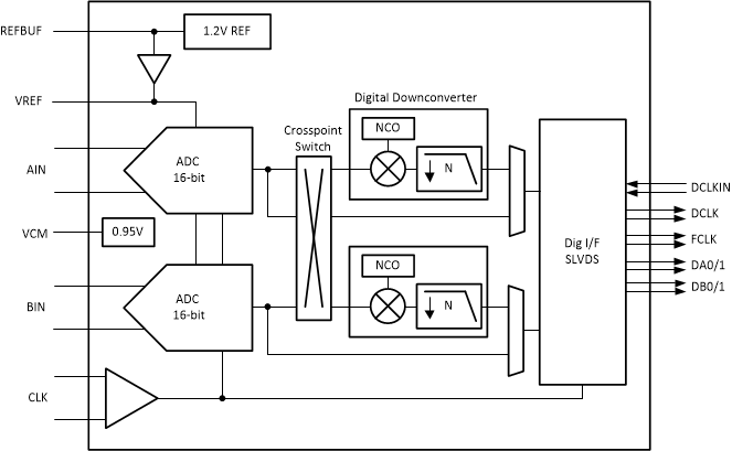
The ADC3661, ADC3662, and ADC3663 (ADC366x) family of devices are low-noise, ultra-low power, 16-bit, 10-MSPS to 65-MSPS, high-speed, dual-channel, analog-to-digital converters (ADCs). Designed for low noise performance, these devices deliver a noise spectral density of –158 dBFS/Hz combined with great linearity and dynamic range. The ADC366x offers good dc precision together with IF sampling support making these devices suitable for a wide range of applications. High-speed control loops benefit from the short latency as low as only 1 clock cycle. The ADC consumes only 94 mW/ch at 65 MSPS and power consumption that scales well with lower sampling rates.

The ADC366x uses a serial LVDS (SLVDS) interface to output the data. The devices support a two-lane, a one-lane and a half-lane option. These devices are a pin-to-pin compatible family with 16-bit and 18-bit resolution and different speed grades. The devices come in a 40-pint QFN package (5 x 5 mm), and supports the extended industrial temperature range of –40°C to +105⁰C.

Package Information
PART NUMBER PACKAGE(1)BODY SIZE (NOM)
ADC366xWQFN (40)5.00 × 5.00 mm
For all available packages, see the orderable addendum at the end of the data sheet.
Table 3-1 Device Comparison
PART NUMBERRESOLUTIONSAMPLING RATE
ADC366116 BIT10 MSPS
ADC366216 BIT25 MSPS
ADC366316 BIT65 MSPS
ADC366414 BIT125 MSPS
GUID-EE66DA3B-BEB3-43DE-8134-B7D7B8E1E002-low.gif Simplified Block Diagram