SBASAV7 January   2024 ADS1014L , ADS1015L

PRODUCTION DATA  

  1.   1
  2. Features
  3. Applications
  4. Description
  5. Device Comparison Table
  6. Pin Configuration and Functions
  7. Specifications
    1. 6.1 Absolute Maximum Ratings
    2. 6.2 ESD Ratings
    3. 6.3 Recommended Operating Conditions
    4. 6.4 Thermal Information
    5. 6.5 Electrical Characteristics
    6. 6.6 I2C Timing Requirements
    7. 6.7 Timing Diagram
  8. Detailed Description
    1. 7.1 Overview
    2. 7.2 Functional Block Diagrams
    3. 7.3 Feature Description
      1. 7.3.1 Multiplexer
      2. 7.3.2 Analog Inputs
      3. 7.3.3 Full-Scale Range (FSR) and LSB Size
      4. 7.3.4 Voltage Reference
      5. 7.3.5 Oscillator
      6. 7.3.6 Output Data Rate and Conversion Time
      7. 7.3.7 Digital Comparator
      8. 7.3.8 Conversion-Ready Pin
      9. 7.3.9 SMBus Alert Response
    4. 7.4 Device Functional Modes
      1. 7.4.1 Reset and Power-Up
      2. 7.4.2 Operating Modes
        1. 7.4.2.1 Single-Shot Mode
        2. 7.4.2.2 Continuous-Conversion Mode
    5. 7.5 Programming
      1. 7.5.1 I2C Interface
        1. 7.5.1.1 I2C Address Selection
        2. 7.5.1.2 I2C Interface Speed
          1. 7.5.1.2.1 Serial Clock (SCL) and Serial Data (SDA)
        3. 7.5.1.3 I2C Data Transfer Protocol
        4. 7.5.1.4 Timeout
        5. 7.5.1.5 I2C General-Call (Software Reset)
      2. 7.5.2 Reading and Writing Register Data
        1. 7.5.2.1 Reading Conversion Data or the Configuration Register
        2. 7.5.2.2 Writing the Configuration Register
      3. 7.5.3 Data Format
  9. Register Map
  10. Application and Implementation
    1. 9.1 Application Information
      1. 9.1.1 Basic Connections
      2. 9.1.2 Unused Inputs and Outputs
      3. 9.1.3 Single-Ended Inputs
      4. 9.1.4 Input Protection
      5. 9.1.5 Analog Input Filtering
      6. 9.1.6 Connecting Multiple Devices
      7. 9.1.7 Duty Cycling For Low Power
      8. 9.1.8 I2C Communication Sequence Example
    2. 9.2 Typical Application
      1. 9.2.1 Design Requirements
      2. 9.2.2 Detailed Design Procedure
      3. 9.2.3 Application Curve
    3. 9.3 Power Supply Recommendations
      1. 9.3.1 Power-Supply Sequencing
      2. 9.3.2 Power-Supply Decoupling
    4. 9.4 Layout
      1. 9.4.1 Layout Guidelines
      2. 9.4.2 Layout Example
  11. 10Device and Documentation Support
    1. 10.1 Receiving Notification of Documentation Updates
    2. 10.2 Support Resources
    3. 10.3 Trademarks
    4. 10.4 Electrostatic Discharge Caution
    5. 10.5 Glossary
  12. 11Revision History
  13. 12Mechanical, Packaging, and Orderable Information

Package Options

Mechanical Data (Package|Pins)
Thermal pad, mechanical data (Package|Pins)
Orderable Information

Data Format

The ADS101xL provides 12 bits of data in binary two's-complement format that is left-justified within the 16-bit Conversion register. A positive full-scale (+FS) input produces an output code of 7FFh and a negative full-scale (–FS) input produces an output code of 800h. The output clips at these codes for signals that exceed full-scale. Table 7-3 summarizes the ideal output codes for different input signals. Figure 7-12 shows code transitions versus input voltage.

Table 7-3 Input Signal Versus Ideal Output Code
INPUT SIGNAL
VIN = (VAINP – VAINN)
IDEAL OUTPUT CODE(1)
≥ +FS (211 – 1) / 211 7FFh
+FS / 211 001h
0 000h
–FS / 211 FFFh
≤ –FS 800h
Excludes the effects of noise, INL, offset, and gain errors.
The D[11:0] bits of the Conversion register are shown.
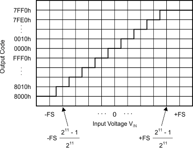
ADS1014L ADS1015L Code
                    Transition Diagram Figure 7-12 Code Transition Diagram
Note:

Single-ended signal measurements, where VAINN = 0 V and VAINP = 0 V to +FS, only use the positive code range from 000h to 7FFh. However, because of device offset, the ADS101xL can still output negative codes if VAINP is close to 0 V.