SBAS741B October   2015  – April 2020 ADS1018-Q1

PRODUCTION DATA.  

  1. Features
  2. Applications
  3. Description
    1.     Device Images
      1.      K-Type Thermocouple Measurement Using Integrated Temperature Sensor for Cold-Junction Compensation
  4. Revision History
  5. Device Comparison Table
  6. Pin Configuration and Functions
    1.     Pin Functions
  7. Specifications
    1. 7.1 Absolute Maximum Ratings
    2. 7.2 ESD Ratings
    3. 7.3 Recommended Operating Conditions
    4. 7.4 Thermal Information
    5. 7.5 Electrical Characteristics
    6. 7.6 Timing Requirements: Serial Interface
    7. 7.7 Switching Characteristics: Serial Interface
    8. 7.8 Typical Characteristics
  8. Detailed Description
    1. 8.1 Overview
    2. 8.2 Functional Block Diagram
    3. 8.3 Feature Description
      1. 8.3.1 Multiplexer
      2. 8.3.2 Analog Inputs
      3. 8.3.3 Full-Scale Range (FSR) and LSB Size
      4. 8.3.4 Voltage Reference
      5. 8.3.5 Oscillator
      6. 8.3.6 Temperature Sensor
        1. 8.3.6.1 Converting from Temperature to Digital Codes
        2. 8.3.6.2 Converting from Digital Codes to Temperature
    4. 8.4 Device Functional Modes
      1. 8.4.1 Reset and Power-Up
      2. 8.4.2 Operating Modes
        1. 8.4.2.1 Single-Shot Mode and Power-Down
        2. 8.4.2.2 Continuous-Conversion Mode
      3. 8.4.3 Duty Cycling for Low Power
    5. 8.5 Programming
      1. 8.5.1 Serial Interface
      2. 8.5.2 Chip Select (CS)
      3. 8.5.3 Serial Clock (SCLK)
      4. 8.5.4 Data Input (DIN)
      5. 8.5.5 Data Output and Data Ready (DOUT/DRDY)
      6. 8.5.6 Data Format
      7. 8.5.7 Data Retrieval
        1. 8.5.7.1 32-Bit Data Transmission Cycle
        2. 8.5.7.2 16-Bit Data Transmission Cycle
    6. 8.6 Register Maps
      1. 8.6.1 Conversion Register [reset = 0000h]
        1. Table 4. Conversion Register Field Descriptions
      2. 8.6.2 Config Register [reset = 058Bh]
        1. Table 5. Config Register Field Descriptions
  9. Application and Implementation
    1. 9.1 Application Information
      1. 9.1.1 Serial Interface Connections
      2. 9.1.2 GPIO Ports for Communication
      3. 9.1.3 Analog Input Filtering
      4. 9.1.4 Single-Ended Inputs
      5. 9.1.5 Connecting Multiple Devices
      6. 9.1.6 Pseudo Code Example
    2. 9.2 Typical Application
      1. 9.2.1 Design Requirements
      2. 9.2.2 Detailed Design Procedure
      3. 9.2.3 Application Curves
  10. 10Power Supply Recommendations
    1. 10.1 Power-Supply Sequencing
    2. 10.2 Power-Supply Decoupling
  11. 11Layout
    1. 11.1 Layout Guidelines
    2. 11.2 Layout Example
  12. 12Device and Documentation Support
    1. 12.1 Documentation Support
      1. 12.1.1 Related Documentation
    2. 12.2 Receiving Notification of Documentation Updates
    3. 12.3 Community Resources
    4. 12.4 Trademarks
    5. 12.5 Electrostatic Discharge Caution
    6. 12.6 Glossary
  13. 13Mechanical, Packaging, and Orderable Information

Package Options

Mechanical Data (Package|Pins)
Thermal pad, mechanical data (Package|Pins)
Orderable Information

Pseudo Code Example

The flow chart in Figure 22 shows a pseudo-code sequence with the required steps to set up communication between the device and a microcontroller to take subsequent readings from the ADS1018-Q1. As an example, the default Config register settings are changed to set up the device for FSR = ±0.512 V, continuous-conversion mode, and a 920-SPS data rate.
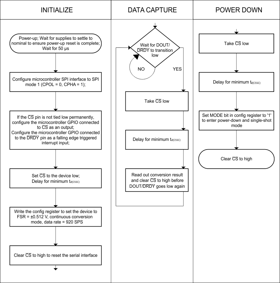
ADS1018-Q1 psuedo-code_sbas741.gifFigure 22. Pseudo-Code Example Flowchart