SBASAV5 December 2023 ADS1114L , ADS1115L
PRODUCTION DATA
- 1
- 1 Features
- 2 Applications
- 3 Description
- 4 Device Comparison Table
- 5 Pin Configuration and Functions
- 6 Specifications
- 7 Parameter Measurement Information
- 8 Detailed Description
- 9 Register Map
- 10Application and Implementation
- 11Device and Documentation Support
- 12Revision History
- 13Mechanical, Packaging, and Orderable Information
Package Options
Mechanical Data (Package|Pins)
- DGS|10
Thermal pad, mechanical data (Package|Pins)
Orderable Information
8.3.2 Analog Inputs
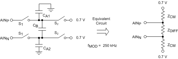
The ADS111xL use a switched-capacitor input stage where capacitors are continuously charged and then discharged to measure the voltage between AINP and AINN. The frequency at which the input signal is sampled is called the sampling frequency or the modulator frequency (fMOD). The ADS111xL has a 1-MHz internal oscillator that is further divided by a factor of 4 to generate fMOD at 250 kHz. The capacitors used in this input stage are small, and to external circuitry, the average loading appears resistive. Figure 8-4 shows this structure. The capacitor values set the resistance and switching rate. Figure 8-5 shows the timing for the switches in Figure 8-4. During the sampling phase, switches S1 are closed. This event charges CA1 to V(AINP), CA2 to V(AINN), and CB to (V(AINP) – V(AINN)). During the discharge phase, S1 is first opened and then S2 is closed. Both CA1 and CA2 then discharge to approximately 0.7 V and CB discharges to 0 V. This charging draws a very small transient current from the source driving the ADS111xL analog inputs. The average value of this current can be used to calculate the effective impedance (Zeff), where Zeff = VIN / IAVERAGE.
 Figure 8-4 Simplified Analog Input Circuit
 Figure 8-5 S1 and S2 Switch Timing
The common-mode input impedance is measured by applying a common-mode signal to the shorted AINP and AINN inputs and measuring the average current consumed by each pin. The common-mode input impedance changes depending on the full-scale range, but is approximately 6 MΩ for the default full-scale range. In Figure 8-4, the common-mode input impedance is ZCM.
The differential input impedance is measured by applying a differential signal to AINP and AINN inputs where one input is held at 0.7 V. The current that flows through the pin connected to 0.7 V is the differential current and scales with the full-scale range. In Figure 8-4, the differential input impedance is ZDIFF.
Make sure to consider the typical value of the input impedance. Unless the input source has a low impedance, the ADS111xL input impedance can affect measurement accuracy. For sources with high-output impedance, buffering can be necessary. Active buffers introduce noise, and also introduce offset and gain errors. Consider all of these factors in high-accuracy applications.
The clock oscillator frequency drifts slightly with temperature; therefore, the input impedances also drift. For most applications, this input impedance drift is negligible, and can be ignored.