SBAS852A August   2017  – February 2020 ADS114S06B , ADS114S08B

PRODUCTION DATA.  

  1. Features
  2. Applications
  3. Description
    1.     Device Images
      1.      Functional Block Diagram
  4. Revision History
  5. Device Comparison Table
  6. Pin Configuration and Functions
    1.     Pin Functions
  7. Specifications
    1. 7.1 Absolute Maximum Ratings
    2. 7.2 ESD Ratings
    3. 7.3 Recommended Operating Conditions
    4. 7.4 Thermal Information
    5. 7.5 Electrical Characteristics
    6. 7.6 Timing Requirements
    7. 7.7 Switching Characteristics
    8. 7.8 Typical Characteristics
  8. Parameter Measurement Information
    1. 8.1 Noise Performance
  9. Detailed Description
    1. 9.1 Overview
    2. 9.2 Functional Block Diagram
    3. 9.3 Feature Description
      1. 9.3.1  Multiplexer
      2. 9.3.2  Low-Noise Programmable Gain Amplifier
        1. 9.3.2.1 PGA Input-Voltage Requirements
        2. 9.3.2.2 Bypassing the PGA
      3. 9.3.3  Voltage Reference
        1. 9.3.3.1 Internal Reference
        2. 9.3.3.2 External Reference
        3. 9.3.3.3 Reference Buffers
      4. 9.3.4  Clock Source
      5. 9.3.5  Delta-Sigma Modulator
      6. 9.3.6  Digital Filter
        1. 9.3.6.1 Digital Filter Frequency Response
        2. 9.3.6.2 Data Conversion Time
        3. 9.3.6.3 Note on Conversion Time
        4. 9.3.6.4 50-Hz and 60-Hz Line Cycle Rejection
      7. 9.3.7  Excitation Current Sources (IDACs)
      8. 9.3.8  Bias Voltage Generation
      9. 9.3.9  System Monitor
        1. 9.3.9.1 Internal Temperature Sensor
        2. 9.3.9.2 Power Supply Monitors
        3. 9.3.9.3 Burn-Out Current Sources
      10. 9.3.10 Status Register
        1. 9.3.10.1 POR Flag
        2. 9.3.10.2 RDY Flag
        3. 9.3.10.3 External Reference Monitor
      11. 9.3.11 General-Purpose Inputs and Outputs (GPIOs)
      12. 9.3.12 Calibration
        1. 9.3.12.1 Offset Calibration
        2. 9.3.12.2 Gain Calibration
    4. 9.4 Device Functional Modes
      1. 9.4.1 Reset
        1. 9.4.1.1 Power-On Reset
        2. 9.4.1.2 RESET Pin
        3. 9.4.1.3 Reset by Command
      2. 9.4.2 Power-Down Mode
      3. 9.4.3 Standby Mode
      4. 9.4.4 Conversion Modes
        1. 9.4.4.1 Continuous Conversion Mode
        2. 9.4.4.2 Single-Shot Conversion Mode
    5. 9.5 Programming
      1. 9.5.1 Serial Interface
        1. 9.5.1.1 Chip Select (CS)
        2. 9.5.1.2 Serial Clock (SCLK)
        3. 9.5.1.3 Serial Data Input (DIN)
        4. 9.5.1.4 Serial Data Output and Data Ready (DOUT/DRDY)
        5. 9.5.1.5 Data Ready (DRDY)
        6. 9.5.1.6 Timeout
      2. 9.5.2 Data Format
      3. 9.5.3 Commands
        1. 9.5.3.1  NOP
        2. 9.5.3.2  WAKEUP
        3. 9.5.3.3  POWERDOWN
        4. 9.5.3.4  RESET
        5. 9.5.3.5  START
        6. 9.5.3.6  STOP
        7. 9.5.3.7  SYOCAL
        8. 9.5.3.8  SYGCAL
        9. 9.5.3.9  SFOCAL
        10. 9.5.3.10 RDATA
        11. 9.5.3.11 RREG
        12. 9.5.3.12 WREG
      4. 9.5.4 Interfacing with Multiple Devices
    6. 9.6 Register Map
      1. 9.6.1 Configuration Registers
      2. 9.6.2 Register Descriptions
        1. 9.6.2.1  Device ID Register (address = 00h) [reset = xxh]
          1. Table 16. Device ID (ID) Register Field Descriptions
        2. 9.6.2.2  Device Status Register (address = 01h) [reset = 80h]
          1. Table 17. Device Status (STATUS) Register Field Descriptions
        3. 9.6.2.3  Input Multiplexer Register (address = 02h) [reset = 01h]
          1. Table 18. Input Multiplexer (INPMUX) Register Field Descriptions
        4. 9.6.2.4  Gain Setting Register (address = 03h) [reset = 00h]
          1. Table 19. Gain Setting (PGA) Register Field Descriptions
        5. 9.6.2.5  Data Rate Register (address = 04h) [reset = 14h]
          1. Table 20. Data Rate (DATARATE) Register Field Descriptions
        6. 9.6.2.6  Reference Control Register (address = 05h) [reset = 10h]
          1. Table 21. Reference Control (REF) Register Field Descriptions
        7. 9.6.2.7  Excitation Current Register 1 (address = 06h) [reset = 00h]
          1. Table 22. Excitation Current Register 1 (IDACMAG) Register Field Descriptions
        8. 9.6.2.8  Excitation Current Register 2 (address = 07h) [reset = FFh]
          1. Table 23. Excitation Current Register 2 (IDACMUX) Register Field Descriptions
        9. 9.6.2.9  Sensor Biasing Register (address = 08h) [reset = 00h]
          1. Table 24. Sensor Biasing (VBIAS) Register Field Descriptions
        10. 9.6.2.10 System Control Register (address = 09h) [reset = 10h]
          1. Table 25. System Control (SYS) Register Field Descriptions
        11. 9.6.2.11 Reserved Register (address = 0Ah) [reset = 00h]
          1. Table 26. Reserved Register Field Descriptions
        12. 9.6.2.12 Offset Calibration Register 1 (address = 0Bh) [reset = 00h]
          1. Table 27. Offset Calibration Register 1 (OFCAL0) Register Field Descriptions
        13. 9.6.2.13 Offset Calibration Register 2 (address = 0Ch) [reset = 00h]
          1. Table 28. Offset Calibration Register 2 (OFCAL1) Register Field Descriptions
        14. 9.6.2.14 Reserved Register (address = 0Dh) [reset = 00h]
          1. Table 29. Reserved Register Field Descriptions
        15. 9.6.2.15 Gain Calibration Register 1 (address = 0Eh) [reset = 00h]
          1. Table 30. Gain Calibration Register 1 (FSCAL0) Field Descriptions
        16. 9.6.2.16 Gain Calibration Register 2 (address = 0Fh) [reset = 40h]
          1. Table 31. Gain Calibration Register 2 (FSCAL1) Field Descriptions
        17. 9.6.2.17 GPIO Data Register (address = 10h) [reset = 00h]
          1. Table 32. GPIO Data (GPIODAT) Register Field Descriptions
        18. 9.6.2.18 GPIO Configuration Register (address = 11h) [reset = 00h]
          1. Table 33. GPIO Configuration (GPIOCON) Register Field Descriptions
  10. 10Application and Implementation
    1. 10.1 Application Information
      1. 10.1.1 Serial Interface Connections
      2. 10.1.2 Analog Input Filtering
      3. 10.1.3 External Reference and Ratiometric Measurements
      4. 10.1.4 Establishing a Proper Input Voltage
      5. 10.1.5 Unused Inputs and Outputs
      6. 10.1.6 Pseudo Code Example
    2. 10.2 Typical Application
      1. 10.2.1 Design Requirements
      2. 10.2.2 Detailed Design Procedure
        1. 10.2.2.1 Register Settings
      3. 10.2.3 Application Curves
    3. 10.3 What To Do and What Not To Do
  11. 11Power Supply Recommendations
    1. 11.1 Power Supplies
    2. 11.2 Power-Supply Sequencing
    3. 11.3 Power-On Reset
    4. 11.4 Power-Supply Decoupling
  12. 12Layout
    1. 12.1 Layout Guidelines
    2. 12.2 Layout Example
  13. 13Device and Documentation Support
    1. 13.1 Device Support
      1. 13.1.1 Development Support
    2. 13.2 Documentation Support
      1. 13.2.1 Related Documentation
    3. 13.3 Related Links
    4. 13.4 Receiving Notification of Documentation Updates
    5. 13.5 Community Resources
    6. 13.6 Trademarks
    7. 13.7 Electrostatic Discharge Caution
    8. 13.8 Glossary
  14. 14Mechanical, Packaging, and Orderable Information

Package Options

Refer to the PDF data sheet for device specific package drawings

Mechanical Data (Package|Pins)
  • RHB|32
  • PBS|32
Thermal pad, mechanical data (Package|Pins)
Orderable Information

Conversion Modes

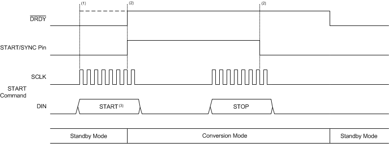
The ADS114S0xB offers two conversion modes: continuous conversion and single-shot conversion mode. Continuous-conversion mode converts indefinitely until stopped by the user. Single-shot conversion mode performs one conversion after the START/SYNC pin is taken high or after the START command is sent. Use the MODE bit in the data rate register (04h) to program the conversion mode. Figure 69 shows how the START/SYNC pin and the START command are used to control ADC conversions.
ADS114S06B ADS114S08B ai_start_stop_sbas660.gif
DRDY rises at the first SCLK rising edge or the rising edge of the START/SYNC pin.
START and STOP commands take effect 2 · tCLK after the seventh SCLK falling edge. The conversion starts 2 · tCLK after the START/SYNC rising edge.
To synchronize a conversion, the STOP command must be issued prior to the START command. STOP and START commands can be issued without a delay between the commands.
Figure 69. Conversion Start and Stop Timing

ADC conversions are controlled by the START/SYNC pin or by serial commands. For the device to start converting in continuous conversion or single-shot conversion mode, a START command must be sent or the START/SYNC pin must be taken high. If using commands to control conversions, keep the START/SYNC pin low to avoid possible contentions between the START/SYNC pin and commands.

Conversions can be synchronized to perform a conversion at a particular time. To synchronize the conversion with the START/SYNC pin, take the pin low. The rising edge of the START/SYNC pin starts a new conversion. Similarly, a conversion can be synchronized using the START command. If the device is in standby mode, issue a START command. If the device is in conversion mode, issue a STOP command followed by a START command. The STOP and START commands can be consecutive. A new conversion starts on the seventh SCLK falling edge of the START command.