SBAS350G June 2005 – January 2021 ADS1232 , ADS1234
PRODUCTION DATA
- 1 Features
- 2 Applications
- 3 Description
- 4 Revision History
- 5 Pin Configuration and Functions
- 6 Specifications
- 7 Parameter Measurement Information
-
8 Detailed Description
- 8.1 Overview
- 8.2 Functional Block Diagram
- 8.3
Feature Description
- 8.3.1 Analog Inputs (AINPX, AINNX)
- 8.3.2 Temperature Sensor (ADS1232 Only)
- 8.3.3 Low-Noise PGA
- 8.3.4 Voltage Reference Inputs (REFP, REFN)
- 8.3.5 Clock Sources
- 8.3.6 Digital Filter Frequency Response
- 8.3.7 Settling Time
- 8.3.8 Data Rate
- 8.3.9 Data Format
- 8.3.10 Data Ready and Data Output (DRDY/DOUT)
- 8.3.11 Serial Clock Input (SCLK)
- 8.3.12 Data Retrieval
- 8.4 Device Functional Modes
- 9 Application and Implementation
- 10Power Supply Recommendations
- 11Layout
- 12Device and Documentation Support
- 13Mechanical, Packaging, and Orderable Information
Package Options
Mechanical Data (Package|Pins)
- PW|28
Thermal pad, mechanical data (Package|Pins)
- PW|28
Orderable Information
3 Description
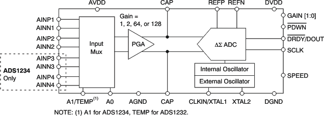
The ADS1232 and ADS1234 (ADS123x) are precision, 24-bit, analog-to-digital converters (ADCs). With a low-noise programmable gain amplifier (PGA), a precision delta-sigma ADC, and internal oscillator, the ADS123x provide a complete front-end solution for bridge sensor applications including weigh scales, strain gauges, and pressure sensors.
An input multiplexer (MUX) accepts either two (ADS1232) or four (ADS1234) differential inputs. The ADS1232 also includes a temperature sensor to monitor ambient temperature. The low-noise PGA has a selectable gain of 1, 2, 64, or 128, supporting a full-scale differential input of ±2.5 V, ±1.25 V, ±39 mV, or ±19.5 mV.
The delta-sigma ADC provides a maximum of 23.5-bits effective resolution, and supports two data rates: 10 SPS (providing 50-Hz and 60-Hz rejection) and 80 SPS. The ADS123x can be clocked externally using an oscillator or a crystal, or by the internal oscillator.
Offset calibration is performed on-demand, and the ADS123x can be put in a low-power standby mode or shut off completely in power-down mode. The ADS123x are operated through simple pin-driven control—there are no digital registers to program.
Data are output over a two-wire serial interface that connects directly to the MSP430 and other microcontrollers.
| PART NUMBER | PACKAGE | BODY SIZE (NOM) |
|---|---|---|
| ADS1232 | TSSOP (24) | 7.80 mm × 4.40 mm |
| ADS1234 | TSSOP (28) | 9.70 mm × 4.40 mm |
 Block Diagram