SBAS760C March   2018  – January 2019 ADS1260 , ADS1261

PRODUCTION DATA.  

  1. Features
  2. Applications
  3. Description
    1.     Device Images
      1.      Block Diagram
  4. Revision History
  5. Device Comparison Table
  6. Pin Configuration and Functions
    1.     Pin Functions
  7. Specifications
    1. 7.1 Absolute Maximum Ratings
    2. 7.2 ESD Ratings
    3. 7.3 Recommended Operating Conditions
    4. 7.4 Thermal Information
    5. 7.5 Electrical Characteristics
    6. 7.6 Timing Requirements
    7. 7.7 Switching Characteristics
    8. 7.8 Typical Characteristics
  8. Parameter Measurement Information
    1. 8.1 Noise Performance
  9. Detailed Description
    1. 9.1 Overview
    2. 9.2 Functional Block Diagram
    3. 9.3 Feature Description
      1. 9.3.1  Analog Inputs
        1. 9.3.1.1 ESD Diodes
        2. 9.3.1.2 Input Multiplexer
        3. 9.3.1.3 Temperature Sensor
        4. 9.3.1.4 Power-Supply Readback
        5. 9.3.1.5 Inputs Open
        6. 9.3.1.6 Internal VCOM Connection
        7. 9.3.1.7 Alternate Functions
      2. 9.3.2  PGA
        1. 9.3.2.1 PGA Bypass Mode
        2. 9.3.2.2 PGA Voltage Monitor
      3. 9.3.3  Reference Voltage
        1. 9.3.3.1 Internal Reference
        2. 9.3.3.2 External Reference
        3. 9.3.3.3 AVDD - AVSS Reference (Default)
        4. 9.3.3.4 Reference Monitor
      4. 9.3.4  Level-Shift Voltage (VBIAS)
      5. 9.3.5  Burn-Out Current Sources
      6. 9.3.6  Sensor-Excitation Current Sources (IDAC1 and IDAC2)
      7. 9.3.7  General-Purpose Input/Outputs (GPIOs)
      8. 9.3.8  Oversampling
      9. 9.3.9  Modulator
      10. 9.3.10 Digital Filter
        1. 9.3.10.1 Sinc Filter
          1. 9.3.10.1.1 Sinc Filter Frequency Response
        2. 9.3.10.2 FIR Filter
          1. 9.3.10.2.1 FIR Filter Frequency Response
        3. 9.3.10.3 Filter Bandwidth
        4. 9.3.10.4 50-Hz and 60-Hz Normal Mode Rejection
    4. 9.4 Device Functional Modes
      1. 9.4.1 Conversion Control
        1. 9.4.1.1 Continuous-Conversion Mode
        2. 9.4.1.2 Pulse-Conversion Mode
        3. 9.4.1.3 Conversion Latency
        4. 9.4.1.4 Start-Conversion Delay
      2. 9.4.2 Chop Mode
      3. 9.4.3 AC-Excitation Mode
      4. 9.4.4 ADC Clock Mode
      5. 9.4.5 Power-Down Mode
        1. 9.4.5.1 Hardware Power-Down
        2. 9.4.5.2 Software Power-Down
      6. 9.4.6 Reset
        1. 9.4.6.1 Power-on Reset
        2. 9.4.6.2 Reset by Pin
        3. 9.4.6.3 Reset by Command
      7. 9.4.7 Calibration
        1. 9.4.7.1 Offset and Full-Scale Calibration
          1. 9.4.7.1.1 Offset Calibration Registers
          2. 9.4.7.1.2 Full-Scale Calibration Registers
        2. 9.4.7.2 Offset Self-Calibration (SFOCAL)
        3. 9.4.7.3 Offset System-Calibration (SYOCAL)
        4. 9.4.7.4 Full-Scale Calibration (GANCAL)
        5. 9.4.7.5 Calibration Command Procedure
        6. 9.4.7.6 User Calibration Procedure
    5. 9.5 Programming
      1. 9.5.1 Serial Interface
        1. 9.5.1.1 Chip Select (CS)
        2. 9.5.1.2 Serial Clock (SCLK)
        3. 9.5.1.3 Data Input (DIN)
        4. 9.5.1.4 Data Output/Data Ready (DOUT/DRDY)
        5. 9.5.1.5 Serial Interface Auto-Reset
      2. 9.5.2 Data Ready (DRDY)
        1. 9.5.2.1 DRDY in Continuous-Conversion Mode
        2. 9.5.2.2 DRDY in Pulse-Conversion Mode
        3. 9.5.2.3 Data Ready by Software Polling
      3. 9.5.3 Conversion Data
        1. 9.5.3.1 Status byte (STATUS)
        2. 9.5.3.2 Conversion Data Format
      4. 9.5.4 CRC
      5. 9.5.5 Commands
        1. 9.5.5.1  NOP Command
        2. 9.5.5.2  RESET Command
        3. 9.5.5.3  START Command
        4. 9.5.5.4  STOP Command
        5. 9.5.5.5  RDATA Command
        6. 9.5.5.6  SYOCAL Command
        7. 9.5.5.7  GANCAL Command
        8. 9.5.5.8  SFOCAL Command
        9. 9.5.5.9  RREG Command
        10. 9.5.5.10 WREG Command
        11. 9.5.5.11 LOCK Command
        12. 9.5.5.12 UNLOCK Command
    6. 9.6 Register Map
      1. 9.6.1  Device Identification (ID) Register (address = 00h) [reset = xxh]
        1. Table 30. ID Register Field Descriptions
      2. 9.6.2  Device Status (STATUS) Register (address = 01h) [reset = 01h]
        1. Table 31. STATUS Register Field Descriptions
      3. 9.6.3  Mode 0 (MODE0) Register (address = 02h) [reset = 24h]
        1. Table 32. MODE0 Register Field Descriptions
      4. 9.6.4  Mode 1 (MODE1) Register (address = 03h) [reset = 01h]
        1. Table 33. MODE1 Register Field Descriptions
      5. 9.6.5  Mode 2 (MODE2) Register (address = 04h) [reset = 00h]
        1. Table 34. MODE2 Register Field Descriptions
      6. 9.6.6  Mode 3 (MODE3) Register (address = 05h) [reset = 00h]
        1. Table 35. MODE3 Register Field Descriptions
      7. 9.6.7  Reference Configuration (REF) Register (address = 06h) [reset = 05h]
        1. Table 36. REF Register Field Descriptions
      8. 9.6.8  Offset Calibration (OFCALx) Registers (address = 07h, 08h, 09h) [reset = 00h, 00h, 00h]
        1. Table 37. OFCAL0, OFCAL1, OFCAL2 Registers Field Description
      9. 9.6.9  Full-Scale Calibration (FSCALx) Registers (address = 0Ah, 0Bh, 0Ch) [reset = 00h, 00h, 40h]
        1. Table 38. FSCAL0, FSCAL1, FSCAL2 Registers Field Description
      10. 9.6.10 IDAC Multiplexer (IMUX) Register (address = 0Dh) [reset = FFh]
        1. Table 39. IMUX Register Field Descriptions
      11. 9.6.11 IDAC Magnitude (IMAG) Register (address = 0Eh) [reset = 00h]
        1. Table 40. IMAG Register Field Descriptions
      12. 9.6.12 Reserved (RESERVED) Register (address = 0Fh) [reset = 00h]
        1. Table 41. RESERVED Register Field Descriptions
      13. 9.6.13 PGA Configuration (PGA) Register (address = 10h) [reset = 00h]
        1. Table 42. PGA Register Field Descriptions
      14. 9.6.14 Input Multiplexer (INPMUX) Register (address = 11h) [reset = FFh]
        1. Table 43. INPMUX Register Field Descriptions
      15. 9.6.15 Input Bias (INPBIAS) Register (address = 12h) [reset = 00h]
        1. Table 44. INPBIAS Register Field Descriptions
  10. 10Application and Implementation
    1. 10.1 Application Information
      1. 10.1.1 Input Range
      2. 10.1.2 Input Overload
      3. 10.1.3 Burn-out Current Source
      4. 10.1.4 Unused Inputs and Outputs
      5. 10.1.5 AC-Excitation
      6. 10.1.6 Serial Interface and Digital Connections
    2. 10.2 Typical Application
      1. 10.2.1 Design Requirements
      2. 10.2.2 Detailed Design Procedure
      3. 10.2.3 Application Curves
    3. 10.3 Initialization Setup
  11. 11Power Supply Recommendations
    1. 11.1 Power-Supply Decoupling
    2. 11.2 Analog Power-Supply Clamp
    3. 11.3 Power-Supply Sequencing
  12. 12Layout
    1. 12.1 Layout Guidelines
    2. 12.2 Layout Example
  13. 13Device and Documentation Support
    1. 13.1 Documentation Support
      1. 13.1.1 Related Documentation
    2. 13.2 Related Links
    3. 13.3 Receiving Notification of Documentation Updates
    4. 13.4 Community Resources
    5. 13.5 Trademarks
    6. 13.6 Electrostatic Discharge Caution
    7. 13.7 Glossary
  14. 14Mechanical, Packaging, and Orderable Information

Package Options

Refer to the PDF data sheet for device specific package drawings

Mechanical Data (Package|Pins)
  • RHB|32
Thermal pad, mechanical data (Package|Pins)
Orderable Information

Typical Application

Figure 99 shows a fault-protected, 3-wire RTD application with hardware-based, lead-wire compensation. Two current sources are used together to compensate the RTD lead wire resistance. One current source (IDAC1) provides excitation to the RTD element through RLEAD1. The reference voltage of the ADC is derived directly from this current by resistor RREF. The second current source cancels lead-wire resistance by generating a voltage drop on lead-wire resistance RLEAD2 equal to the voltage drop of RLEAD1. Because the RRTD signal voltage is measured differentially via inputs AIN2 and AIN3, the voltages across the lead wire resistance cancel. Resistor RBIAS level-shifts the RTD signal voltage to within the ADC input range. The current sources route to the RTD element through low VF diodes to provide input fault protection.
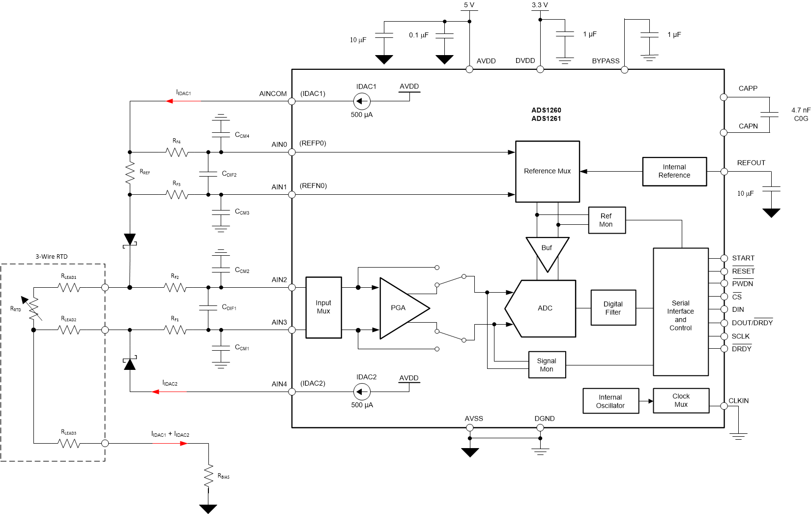
ADS1260 ADS1261 ai_3W_RTD_example_sbas760.gifFigure 99. RTD Element With 3-Wire Lead Resistance Compensation