SBAS691B March 2016 – October 2018 ADS1282-SP
PRODUCTION DATA.
- 1 Features
- 2 Applications
- 3 Description
- 4 Revision History
- 5 Description (continued)
- 6 Pin Configuration and Functions
-
7 Specifications
- 7.1 Absolute Maximum Ratings
- 7.2 ESD Ratings
- 7.3 Recommended Operating Conditions
- 7.4 Thermal Information
- 7.5 Electrical Characteristics
- 7.6 Timing Requirements
- 7.7 Pulse-Sync Timing Requirements
- 7.8 Reset Timing Requirements
- 7.9 Read Data Timing Requirements
- 7.10 Switching Characteristics
- 7.11 Typical Characteristics
-
8 Detailed Description
- 8.1 Overview
- 8.2 Functional Block Diagram
- 8.3
Feature Description
- 8.3.1 Noise Performance
- 8.3.2 Input-Referred Noise
- 8.3.3 Idle Tones
- 8.3.4 Operating Mode
- 8.3.5 Analog Inputs and Multiplexer
- 8.3.6 PGA (Programmable Gain Amplifier)
- 8.3.7 ADC
- 8.3.8 Modulator
- 8.3.9 Modulator Over-Range
- 8.3.10 Modulator Input Impedance
- 8.3.11 Modulator Over-Range Detection (MFLAG)
- 8.3.12 Voltage Reference Inputs (VREFP, VREFN)
- 8.3.13 Digital Filter
- 8.3.14 Master Clock Input (CLK)
- 8.3.15 Synchronization (SYNC Pin and Sync Command)
- 8.3.16 Pulse-Sync Mode
- 8.3.17 Continuous-Sync Mode
- 8.3.18 Reset (RESET Pin and Reset Command)
- 8.3.19 Power-Down (PWDN Pin and Standby Command)
- 8.3.20 Power-On Sequence
- 8.3.21 Serial Interface
- 8.3.22 Data Format
- 8.3.23 Reading Data
- 8.3.24 One-Shot Operation
- 8.4 Device Functional Modes
- 8.5
Programming
- 8.5.1
Commands
- 8.5.1.1 WAKEUP: Wake-Up from Standby Mode
- 8.5.1.2 STANDBY: Standby Mode
- 8.5.1.3 SYNC: Synchronize the A/D Conversion
- 8.5.1.4 RESET: Reset the Device
- 8.5.1.5 RDATAC: Read Data Continuous
- 8.5.1.6 SDATAC: Stop Read Data Continuous
- 8.5.1.7 RDATA: Read Data By Command
- 8.5.1.8 RREG: Read Register Data
- 8.5.1.9 WREG: Write to Register
- 8.5.1.10 OFSCAL: Offset Calibration
- 8.5.1.11 GANCAL: Gain Calibration
- 8.5.2 Calibration Commands
- 8.5.3 User Calibration
- 8.5.4 Configuration Guide
- 8.5.1
Commands
- 8.6 Register Maps
- 9 Application and Implementation
- 10Power Supply Recommendations
- 11Layout
- 12Device and Documentation Support
- 13Mechanical, Packaging, and Orderable Information
Package Options
Mechanical Data (Package|Pins)
- HKV|28
Thermal pad, mechanical data (Package|Pins)
Orderable Information
10 Power Supply Recommendations
Bypass all supply pins with 1-μF ceramic capacitors. In order to minimize the lead and trace inductance, place the capacitors as close to the supply pins as possible. Where double-sided component mounting is allowed, these capacitors are best placed directly under the package. In addition to power supplies, the device has a reference supply at pins VREFP and VREFN that should also be bypassed. Bypass these pins with at least a 1-μF capacitor as higher value capacitors yield superior low-frequency noise suppression. For best results, choose low-inductance ceramic chip capacitors and place as close as possible to the device pins.
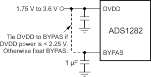
The DVDD power supply operates over the range of 1.75 to 3.6 V. If DVDD is operated at less than 2.25 V, connect the DVDD pin to the BYPAS pin. If DVDD is greater than or equal to 2.25 V, do not connect DVDD to the BYPAS pin. Figure 81 shows this connection.
 Figure 81. DVDD Power