SGLS378G March 2008 – October 2017 ADS5463-SP
PRODUCTION DATA.
- 1 Features
- 2 Applications
- 3 Description
- 4 Revision History
- 5 Pin Configuration and Functions
-
6 Specifications
- 6.1 Absolute Maximum Ratings
- 6.2 ESD Ratings
- 6.3 Recommended Operating Conditions
- 6.4 Thermal Information
- 6.5 Electrical Characteristics: ADS5463-RHA
- 6.6 Electrical Characteristics: ADS5463-RHA
- 6.7 Electrical Characteristics: ADS5463-RHA
- 6.8 Electrical Characteristics: ADS5463-SP
- 6.9 Electrical Characteristics: ADS5463-SP
- 6.10 Electrical Characteristics: ADS5463-SP
- 6.11 Timing Requirements
- 6.12 Typical Characteristics
- 7 Detailed Description
- 8 Application and Implementation
- 9 Power Supply Recommendations
- 10Layout
- 11Device and Documentation Support
- 12Mechanical, Packaging, and Orderable Information
Package Options
Mechanical Data (Package|Pins)
- HFG|84
Thermal pad, mechanical data (Package|Pins)
Orderable Information
5 Pin Configuration and Functions
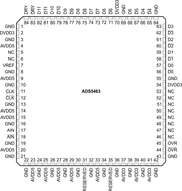
HFG Package
84-Pin CFP
Top View

Pin Functions
| PIN | DESCRIPTION | |
|---|---|---|
| NAME | NO. | |
| AIN | 17 | Differential input signal (positive). |
| AIN | 18 | Differential input signal (negative). |
| AVDD5 | 4, 9, 14, 15, 20, 23, 25, 27, 29, 33 | Analog power supply (5 V). |
| AVDD3 | 37, 39, 41 | Analog power supply (3.3 V) (Suggestion for 250 MSPS: leave option to connect to 5 V for ADS5440/4 compatibility). |
| DVDD3 | 2, 54, 70 | Output driver power supply (3.3 V). |
| GND | 1, 3, 8, 10, 13, 16, 19, 21, 22, 24, 26, 28, 30, 32, 34, 36, 38, 40, 42, 43, 55, 64, 69 | Ground. |
| CLK | 11 | Differential input clock (positive). Conversion initiated on rising edge. |
| CLK | 12 | Differential input clock (negative). |
| D0, D0 | 56, 57 | LVDS digital output pair, least-significant bit (LSB). |
| D1-D3, D1-D3 |
58–63 | LVDS digital output pair. |
| D4–D5, D4–D5 |
65–68 | LVDS digital output pairs. |
| D6–D10, D6–D10 |
71–80 | LVDS digital output pairs. |
| D11, D11 | 81, 82 | LVDS digital output pair, most-significant bit (MSB). |
| DRY, DRY | 83, 84 | Data ready LVDS output pair. |
| NC | 5–6, 46–53 | No connect (5 and 6 should be left floating, 46–53 are possible future bit additions for this pinout and therefore can be connected to a digital bus or left floating). |
| OVR, OVR | 44, 45 | Overrange indicator LVDS output. A logic high signals an analog input in excess of the full-scale range. |
| RESERVED | 31, 35 | Reserved for possible future control features. |
| VREF | 7 | Reference voltage. |