SLAS525D July 2007 – December 2017 ADS5474
PRODUCTION DATA.
- 1 Features
- 2 Applications
- 3 Description
- 4 Revision History
- 5 Pin Configuration and Functions
- 6 Specifications
- 7 Detailed Description
- 8 Application and Implementation
- 9 Power Supply Recommendations
- 10Layout
- 11Device and Documentation Support
- 12Mechanical, Packaging, and Orderable Information
Package Options
Mechanical Data (Package|Pins)
- PFP|80
Thermal pad, mechanical data (Package|Pins)
- PFP|80
Orderable Information
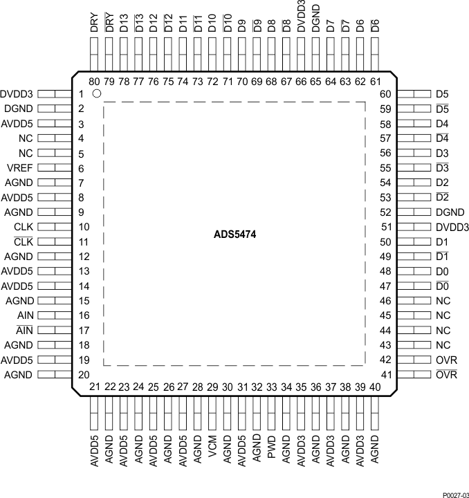
5 Pin Configuration and Functions
Pin Functions
| PIN | DESCRIPTION | ||
|---|---|---|---|
| NAME | NO. | TYPE | |
| AIN | 16 | I | Differential input signal (positive) |
| AIN | 17 | I | Differential input signal (negative) |
| AVDD5 | 3 | Analog power supply (5 V) | |
| 8 | |||
| 13 | |||
| 14 | |||
| 19 | |||
| 21 | |||
| 23 | |||
| 25 | |||
| 27 | |||
| 31 | |||
| AVDD3 | 35 | Analog power supply (3.3 V) (suggestion for ≤ 250 MSPS: leave option to connect to 5 V for ADS5440, ADS5444 13-bit compatibility) | |
| 37 | |||
| 39 | |||
| DVDD3 | 1 | Digital and output driver power supply (3.3 V) | |
| 51 | |||
| 66 | |||
| AGND | 7 | Analog Ground | |
| 9 | |||
| 12 | |||
| 15 | |||
| 18 | |||
| 20 | |||
| 22 | |||
| 24 | |||
| 26 | |||
| 28 | |||
| 30 | |||
| 32 | |||
| 34 | |||
| 36 | |||
| 38 | |||
| 40 | |||
| DGND | 2 | Digital Ground | |
| 52 | |||
| 65 | |||
| CLK | 10 | I | Differential input clock (positive). Conversion is initiated on rising edge, digital outputs on falling edge. |
| CLK | 11 | I | Differential input clock (negative) |
| D0 | 48 | O | LVDS digital output pair, least significant bit (LSB) |
| D0 | 47 | ||
| D1 | 50 | O | LVDS digital output pairs |
| D1 | 49 | ||
| D2 | 54 | ||
| D2 | 53 | ||
| D3 | 56 | ||
| D3 | 55 | ||
| D4 | 58 | ||
| D4 | 57 | ||
| D5 | 60 | ||
| D5 | 59 | ||
| D6 | 62 | ||
| D6 | 61 | ||
| D7 | 64 | ||
| D7 | 63 | ||
| D8 | 68 | ||
| D8 | 67 | ||
| D9 | 70 | ||
| D9 | 69 | ||
| D10 | 72 | ||
| D10 | 71 | ||
| D11 | 74 | ||
| D11 | 73 | ||
| D12 | 76 | ||
| D12 | 75 | ||
| D13 | 78 | O | LVDS digital output pair, most significant bit (MSB) |
| D13 | 77 | ||
| DRY | 80 | O | Data ready LVDS output pair |
| DRY | 79 | ||
| NC | 4 | - | No connection (pins 4 and 5 should be left floating) |
| 5 | |||
| 43 | - | No connection (pins 43 to 46 are possible future bit additions for this pinout and therefore can be connected to a digital bus or left floating) | |
| 44 | |||
| 45 | |||
| 46 | |||
| OVR | 42 | O | Overrange indicator LVDS output. A logic high signals an analog input in excess of the full-scale range. |
| OVR | 41 | ||
| VCM | 29 | O | Common-mode voltage output (3.1 V nominal). Commonly used in DC-coupled applications to set the input signal to the correct common-mode voltage. A 0.1-μF capacitor from VCM to AGND is recommended, but not required. (This pin is not used on the ADS5440, ADS5444, and ADS5463) |
| PWD | 33 | Power-down (active high). Device is in sleep mode when PWD pin is logic HIGH. ADC converter is awake when PWD is logic LOW (grounded). (This pin is not used on the ADS5440, ADS5444, and ADS5463) |
|
| VREF | 6 | Reference voltage input/output (2.4 V nominal). A 0.1-μF capacitor from VREF to AGND is recommended, but not required. | |
| (Power Pad) | (not numbered) | Power Pad for thermal relief, also Analog Ground | |
