SLAS525D July 2007 – December 2017 ADS5474
PRODUCTION DATA.
- 1 Features
- 2 Applications
- 3 Description
- 4 Revision History
- 5 Pin Configuration and Functions
- 6 Specifications
- 7 Detailed Description
- 8 Application and Implementation
- 9 Power Supply Recommendations
- 10Layout
- 11Device and Documentation Support
- 12Mechanical, Packaging, and Orderable Information
Package Options
Mechanical Data (Package|Pins)
- PFP|80
Thermal pad, mechanical data (Package|Pins)
- PFP|80
Orderable Information
6 Specifications
6.1 Absolute Maximum Ratings
over operating free-air temperature range, unless otherwise noted.(1)| MIN | MAX | UNIT | ||
|---|---|---|---|---|
| Supply voltage | AVDD5 to GND | 6 | V | |
| AVDD3 to GND | 5 | |||
| DVDD3 to GND | 5 | |||
| Analog input to GND | Valid when supplies are on and within normal ranges. See additional information in the Power Supplies portion of the applications information in the back of the datasheet regarding Clock and Analog Inputs when the supplies are off. | –0.3 | (AVDD5 + 0.3) | V |
| Clock input to GND | –0.3 | (AVDD5 + 0.3) | V | |
| CLK to CLK | –2.5 | 2.5 | V | |
| Digital data output to GND | –0.3 | (DVDD3 + 0.3) | V | |
| Operating temperature range | –40 | 85 | °C | |
| Maximum junction temperature | +150 | °C | ||
| Storage temperature range | –65 | 150 | °C | |
(1) Stresses beyond those listed under Absolute Maximum Ratings may cause permanent damage to the device. These are stress ratings only, which do not imply functional operation of the device at these or any other conditions beyond those indicated under Recommended Operating Conditions. Exposure to absolute-maximum-rated conditions for extended periods may affect device reliability.
6.2 ESD Ratings
| VALUE | UNIT | |||
|---|---|---|---|---|
| V(ESD) | Electrostatic discharge | Human-body model (HBM), per ANSI/ESDA/JEDEC JS-001(1) | 2000 | V |
(1) JEDEC document JEP155 states that 500-V HBM allows safe manufacturing with a standard ESD control process.
6.3 Recommended Operating Conditions
| MIN | NOM | MAX | UNIT | ||
|---|---|---|---|---|---|
| SUPPLIES | |||||
| AVDD5 | Analog supply voltage | 4.75 | 5 | 5.25 | V |
| AVDD3 | Analog supply voltage | 3.1 | 3.3 | 3.6 | V |
| DVDD3 | Output driver supply voltage | 3 | 3.3 | 3.6 | V |
| ANALOG INPUT | |||||
| Differential input range | 2.2 | VPP | |||
| VCM | Input common mode | 3.1 | V | ||
| DIGITAL OUTPUT (DRY, DATA, OVR) | |||||
| Maximum differential output load | 10 | pF | |||
| CLOCK INPUT (CLK) | |||||
| CLK input sample rate (sine wave) | 20 | 404 | MSPS | ||
| Clock amplitude, differential sine wave (see Figure 37) | 0.5 | 5 | VPP | ||
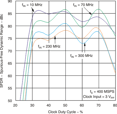
| Clock duty cycle (see Figure 31) | 40% | 50% | 60% | ||
| TA | Operating free-air temperature | –40 | +85 | °C | |
6.4 Thermal Information
| THERMAL METRIC(1) | ADS5474 | UNIT | |
|---|---|---|---|
| PFP (HTQFP) | |||
| 80 PINS | |||
| RθJA | Junction-to-ambient thermal resistance | 25.9 | °C/W |
| RθJC(top) | Junction-to-case (top) thermal resistance | 7.6 | °C/W |
| RθJB | Junction-to-board thermal resistance | 9.8 | °C/W |
| ψJT | Junction-to-top characterization parameter | 0.2 | °C/W |
| ψJB | Junction-to-board characterization parameter | 9.7 | °C/W |
| RθJC(bot) | Junction-to-case (bottom) thermal resistance | 0.2 | °C/W |
(1) For more information about traditional and new thermal metrics, see the Semiconductor and IC Package Thermal Metrics application report.
6.5 Electrical Characteristics
Typical values at TA = 25°C: minimum and maximum values over full temperature range TMIN = –40°C to TMAX = 85°C, sampling rate = 400 MSPS, 50% clock duty cycle, AVDD5 = 5 V, AVDD3 = 3.3 V, DVDD3 = 3.3 V, –1 dBFS differential input, and 3-VPP differential clock, unless otherwise noted.| PARAMETER | TEST CONDITIONS | MIN | TYP | MAX | UNIT | |
|---|---|---|---|---|---|---|
| Resolution | 14 | Bits | ||||
| ANALOG INPUTS | ||||||
| Differential input range | 2.2 | VPP | ||||
| Analog input common-mode voltage | Self-biased; see VCM specification below | 3.1 | V | |||
| Input resistance (dc) | Each input to VCM | 500 | Ω | |||
| Input capacitance | Each input to GND | 2.3 | pF | |||
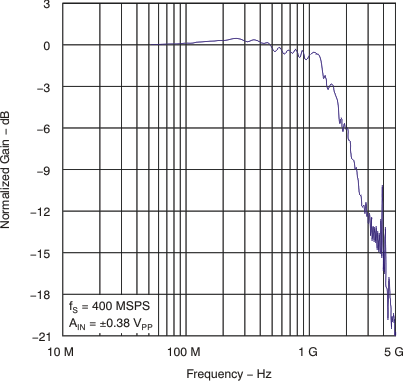
| Analog input bandwidth (–3dB) | 1.44 | GHz | ||||
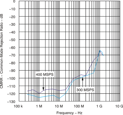
| CMRR | Common-mode rejection ratio | Common-mode signal < 50 MHz (see Figure 27) |
100 | dB | ||
| INTERNAL REFERENCE VOLTAGE | ||||||
| VREF | Reference voltage | 2.4 | V | |||
| VCM | Analog input common-mode voltage reference output | With internal VREF. Provided as an output via the VCM pin for dc-coupled applications. If an external VREF is used, the VCM pin tracks as illustrated in Figure 42 | 2.9 | 3.1 | 3.3 | V |
| VCM temperature coefficient | –0.8 | mV/°C | ||||
| DYNAMIC ACCURACY | ||||||
| No missing codes | Assured | |||||
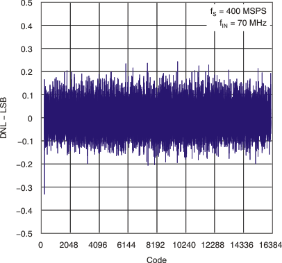
| DNL | Differential linearity error | fIN = 70 MHz | –0.99 | ±0.7 | 1.5 | LSB |
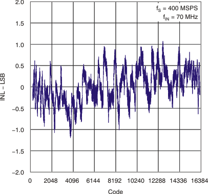
| INL | Integral linearity error | fIN = 70 MHz | –3 | ±1 | 3 | LSB |
| Offset error | –11 | 11 | mV | |||
| Offset temperature coefficient | 0.02 | mV/°C | ||||
| Gain error | –5 | 5 | %FS | |||
| Gain temperature coefficient | –0.02 | %FS/°C | ||||
| POWER SUPPLY | ||||||
| IAVDD5 | 5-V analog supply current | VIN = full-scale, fIN = 70 MHz, fS = 400 MSPS |
338 | 372 | mA | |
| IAVDD3 | 3.3-V analog supply current | VIN = full-scale, fIN = 70 MHz, fS = 400 MSPS |
185 | 201 | mA | |
| IDVDD3 | 3.3-V digital supply current (includes LVDS) |
VIN = full-scale, fIN = 70 MHz, fS = 400 MSPS |
75 | 83 | mA | |
| Total power dissipation | 2.5 | 2.797 | W | |||
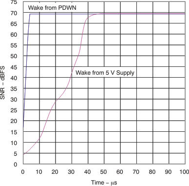
| Power-up time | From turn-on of AVDD5 | 50 | μs | |||
| Wake-up time | From PWD pin switched from HIGH (PWD active) to LOW (ADC awake) (see Figure 28) |
5 | μs | |||
| Power-down power dissipation | PWD pin = logic HIGH | 50 | 350 | mW | ||
| PSRR | Power-supply rejection ratio, AVDD5 supply |
Without 0.1-μF board supply capacitors, with < 1-MHz supply noise (see Figure 46) | 75 | dB | ||
| PSRR | Power-supply rejection ratio, AVDD3 supply |
Without 0.1-μF board supply capacitors, with < 1-MHz supply noise (see Figure 46) | 90 | dB | ||
| PSRR | Power-supply rejection ratio, DVDD3 supply |
Without 0.1-μF board supply capacitors, with < 1-MHz supply noise (see Figure 46) | 110 | dB | ||
| DYNAMIC AC CHARACTERISTICS | ||||||
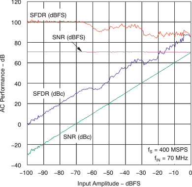
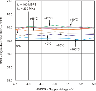
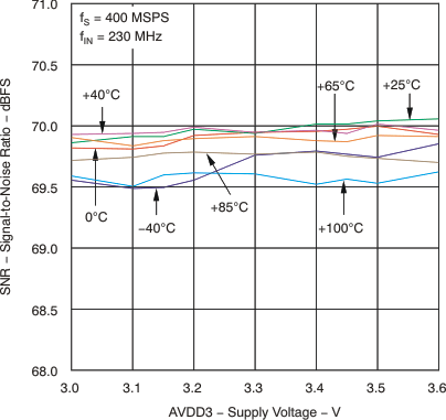
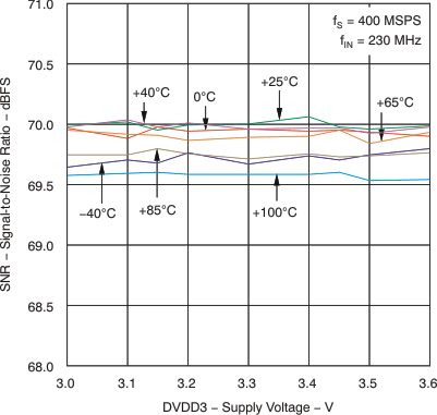
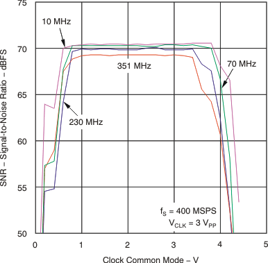
| SNR | Signal-to-noise ratio | fIN = 30 MHz | 70.3 | dBFS | ||
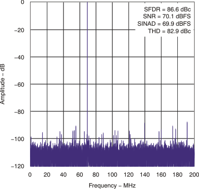
| fIN = 70 MHz | 68.3 | 70.2 | ||||
| fIN = 130 MHz | 70.1 | |||||
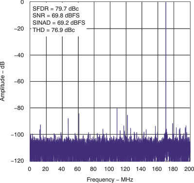
| fIN = 230 MHz | 68 | 69.8 | ||||
| fIN = 351 MHz | 69.1 | |||||
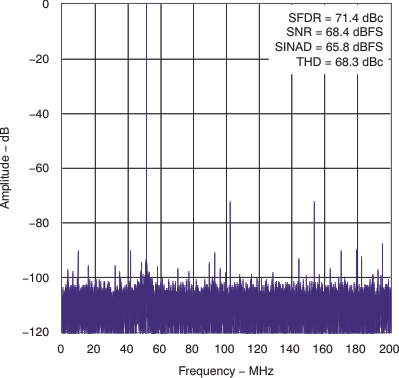
| fIN = 451 MHz | 68.4 | |||||
| fIN = 651 MHz | 67.5 | |||||
| fIN = 751 MHz | 66.6 | |||||
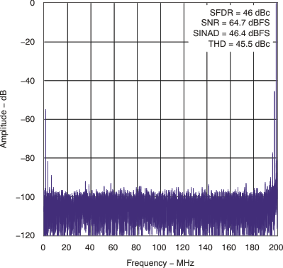
| fIN = 999 MHz | 64.7 | |||||
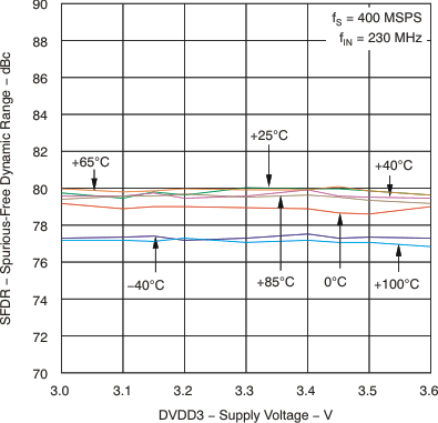
| SFDR | Spurious-free dynamic range | fIN = 30 MHz | 88 | dBc | ||
| fIN = 70 MHz | 74 | 86 | ||||
| fIN = 130 MHz | 80 | |||||
| fIN = 230 MHz | 71 | 80 | ||||
| fIN = 351 MHz | 76 | |||||
| fIN = 451 MHz | 71 | |||||
| fIN = 651 MHz | 60 | |||||
| fIN = 751 MHz | 55 | |||||
| fIN = 999 MHz | 46 | |||||
| HD2 | Second-harmonic | fIN = 30 MHz | 89 | dBc | ||
| fIN = 70 MHz | 87 | |||||
| fIN = 130 MHz | 90 | |||||
| fIN = 230 MHz | 84 | |||||
| fIN = 351 MHz | 76 | |||||
| fIN = 451 MHz | 71 | |||||
| fIN = 651 MHz | 74 | |||||
| fIN = 751 MHz | 70 | |||||
| fIN = 999 MHz | 55 | |||||
| HD3 | Third-harmonic | fIN = 30 MHz | 93 | dBc | ||
| fIN = 70 MHz | 86 | |||||
| fIN = 130 MHz | 80 | |||||
| fIN = 230 MHz | 80 | |||||
| fIN = 351 MHz | 85 | |||||
| fIN = 451 MHz | 71 | |||||
| fIN = 651 MHz | 60 | |||||
| fIN = 751 MHz | 55 | |||||
| fIN = 999 MHz | 46 | |||||
| Worst harmonic, spur (other than HD2 and HD3) |
fIN = 30 MHz | 95 | dBc | |||
| fIN = 70 MHz | 93 | |||||
| fIN = 130 MHz | 85 | |||||
| fIN = 230 MHz | 85 | |||||
| fIN = 351 MHz | 87 | |||||
| fIN = 451 MHz | 87 | |||||
| fIN = 651 MHz | 90 | |||||
| fIN = 751 MHz | 87 | |||||
| fIN = 999 MHz | 80 | |||||
| THD | Total harmonic distortion | fIN = 30 MHz | 86 | dBc | ||
| fIN = 70 MHz | 83 | |||||
| fIN = 130 MHz | 78 | |||||
| fIN = 230 MHz | 77 | |||||
| fIN = 351 MHz | 75 | |||||
| fIN = 451 MHz | 68 | |||||
| fIN = 651 MHz | 60 | |||||
| fIN = 751 MHz | 55 | |||||
| fIN = 999 MHz | 45 | |||||
| SINAD | Signal-to-noise and distortion | fIN = 30 MHz | 69.2 | dBc | ||
| fIN = 70 MHz | 67 | 68.9 | ||||
| fIN = 130 MHz | 68.5 | |||||
| fIN = 230 MHz | 65.5 | 68.2 | ||||
| fIN = 351 MHz | 67.3 | |||||
| fIN = 451 MHz | 64.8 | |||||
| fIN = 651 MHz | 58.5 | |||||
| fIN = 751 MHz | 54 | |||||
| fIN = 999 MHz | 45.4 | |||||
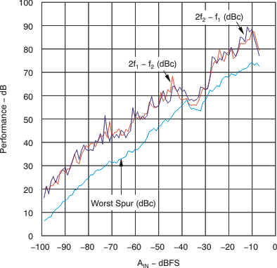
| Two-tone SFDR | fIN1 = 69 MHz, fIN2 = 70 MHz, each tone at –7 dBFS |
93 | dBFS | |||
| fIN1 = 69 MHz, fIN2 = 70 MHz, each tone at –16 dBFS |
95 | |||||
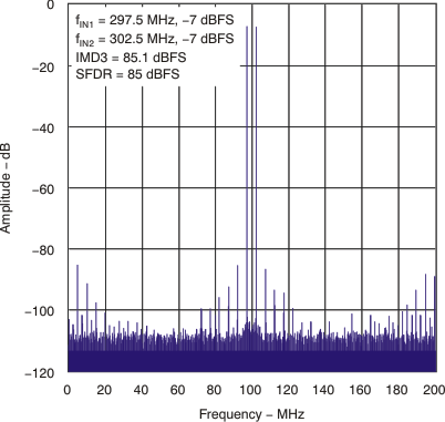
| fIN1 = 297.5 MHz, fIN2 = 302.5 MHz, each tone at –7 dBFS |
85 | |||||
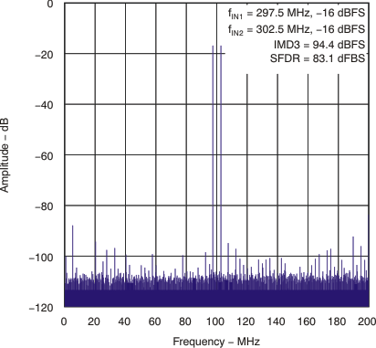
| fIN1 = 297.5 MHz, fIN2 = 302.5 MHz, each tone at –16 dBFS |
83 | |||||
| ENOB | Effective number of bits | fIN = 70 MHz | 10.8 | 11.2 | Bits | |
| fIN = 230 MHz | 10.6 | 10.9 | ||||
| RMS idle-channel noise | Inputs tied to common-mode | 1.8 | LSB | |||
| DIGITAL OUTPUTS | ||||||
| VOD | Differential output voltage (±) | 247 | 350 | 454 | mV | |
| VOC | Common-mode output voltage | 1.125 | 1.375 | V | ||
| DIGITAL INPUTS | ||||||
| VIH | High level input voltage | PWD (pin 33) | 2 | V | ||
| VIL | Low level input voltage | PWD (pin 33) | 0.8 | V | ||
| IIH | High level input current | PWD (pin 33) | 1 | μA | ||
| IIL | Low level input current | PWD (pin 33) | –1 | μA | ||
| Input capacitance | PWD (pin 33) | 2 | pF | |||
6.6 Timing Characteristics
Typical values at TA = 25°C: minimum and maximum values over full temperature range TMIN = –40°C to TMAX = 85°C, sampling rate = 400 MSPS, 50% clock duty cycle, AVDD5 = 5 V, AVDD3 = 3.3 V, DVDD3 = 3.3 V, and 3-VPP differential clock, unless otherwise noted.(1)| TEST CONDITIONS | MIN | NOM | MAX | UNIT | ||
|---|---|---|---|---|---|---|
| ta | Aperture delay | 200 | ps | |||
| Aperture jitter, rms | Internal jitter of the ADC | 103 | fs | |||
| Latency | 3.5 | cycles | ||||
| tCLK | Clock period | 2.5 | 50 | ns | ||
| tCLKH | Clock pulse duration, high | 1 | ns | |||
| tCLKL | Clock pulse duration, low | 1 | ns | |||
| tDRY | CLK to DRY delay(2) | Zero crossing, 10-pF parasitic loading to GND on each output pin | 1000 | 1400 | 1800 | ps |
| tDATA | CLK to DATA/OVR delay(2) | Zero crossing, 10-pF parasitic loading to GND on each output pin | 800 | 1400 | 2000 | ps |
| tSKEW | DATA to DRY skew | tDATA – tDRY, 10-pF parasitic loading to GND on each output pin | –500 | 0 | 500 | ps |
| tRISE | DRY/DATA/OVR rise time | 10-pF parasitic loading to GND on each output pin | 500 | ps | ||
| tFALL | DRY/DATA/OVR fall time | 10-pF parasitic loading to GND on each output pin | 500 | ps | ||
(1) Timing parameters are ensured by design or characterization, but not production tested.
(2) DRY, DATA, and OVR are updated on the falling edge of CLK. The latency must be added to tDATA to determine the overall propagation delay.
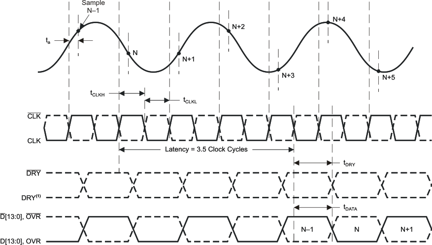
1. Polarity of DRY is undetermined. For further information, see the Digital Outputs section.
Figure 1. Timing Diagram
6.7 Typical Characteristics
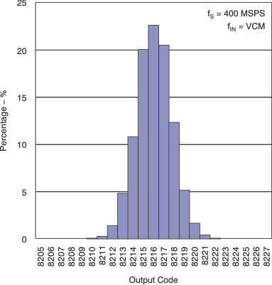
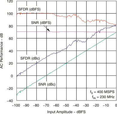
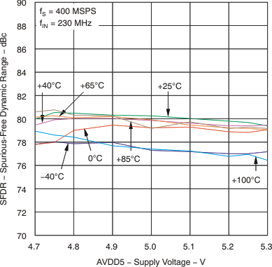
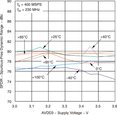
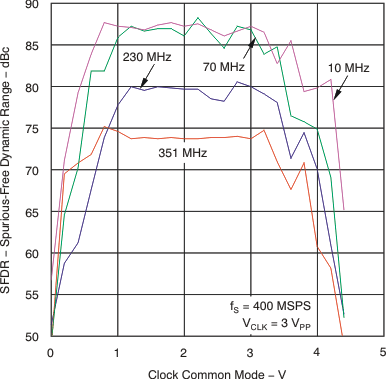
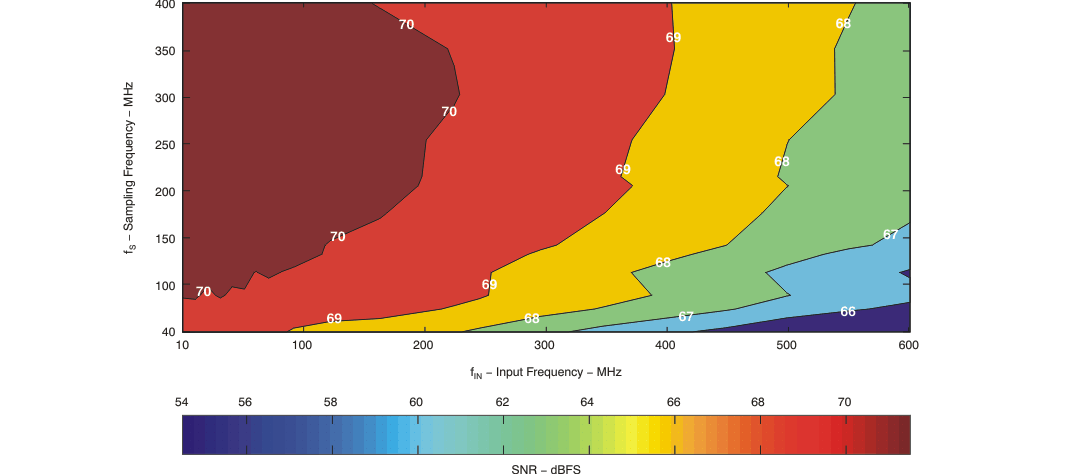
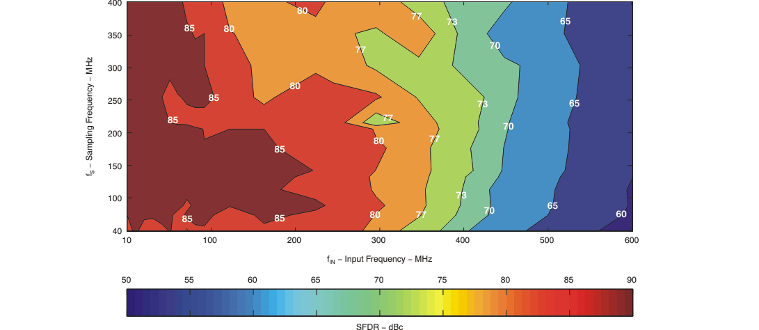
At TA = 25°C, sampling rate = 400 MSPS, 50% clock duty cycle, 3-VPP differential sinusoidal clock, analog input amplitude = –1 dBFS, AVDD5 = 5 V, AVDD3 = 3.3 V, and DVDD3 = 3.3 V, unless otherwise noted.
