SBAS681D November 2014 – December 2015 ADS7043
PRODUCTION DATA.
- 1 Features
- 2 Applications
- 3 Description
- 4 Revision History
- 5 Pin Configuration and Functions
- 6 Specifications
- 7 Parameter Measurement Information
- 8 Detailed Description
- 9 Application and Implementation
- 10Power-Supply Recommendations
- 11Layout
- 12Device and Documentation Support
- 13Mechanical, Packaging, and Orderable Information
Package Options
Refer to the PDF data sheet for device specific package drawings
Mechanical Data (Package|Pins)
- DCU|8
- RUG|8
Thermal pad, mechanical data (Package|Pins)
Orderable Information
8 Detailed Description
8.1 Overview
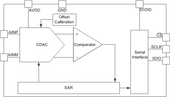
The ADS7043 is an ultralow-power, ultra-small analog-to-digital converter (ADC) that supports a wide analog input range. The analog input range for the device is defined by the AVDD supply voltage. The device samples the input voltage across the AINP and AINM pins on the CS falling edge and starts the conversion. The clock provided on the SCLK pin is used for conversion and data transfer. During conversions, both the AINP and AINM pins are disconnected from the sampling circuit. After the conversion completes, the sampling capacitors are reconnected across the AINP and AINM pins and the device enters acquisition phase.
The device has an internal offset calibration. The offset calibration can be initiated by the user either on power-up or during normal operation; see the Offset Calibration section for more details.
The device also provides a simple serial interface to the host controller and operates over a wide range of digital power supplies. The device requires only a 16-MHz SCLK for supporting a throughput of 1 MSPS. The digital interface also complies with the JESD8-7A (normal range) standard. The Functional Block Diagram section provides a block diagram of the device.
8.2 Functional Block Diagram
8.3 Feature Description
8.3.1 Reference
The device uses the analog supply voltage (AVDD) as a reference, as shown in Figure 32. TI recommends decoupling the AVDD pin with a 1-µF, low equivalent series resistance (ESR) ceramic capacitor. The minimum capacitor value required for AVDD is 200 nF. The AVDD pin functions as a switched capacitor load to the source powering AVDD. The decoupling capacitor provides the instantaneous charge required by the internal circuit and helps in maintaining a stable dc voltage on the AVDD pin. TI recommends powering the AVDD pin with a low output impedance and low-noise regulator (such as the TPS79101).
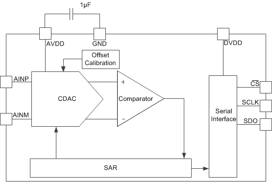 Figure 32. Reference for the Device
8.3.2 Analog Input
The device supports pseudo-differential analog inputs. The ADC samples the difference between AINP and AINM and converts for this voltage. The device is capable of accepting a signal from AVDD / 2 – 100 mV to AVDD / 2 + 100 mV on the AINM input and a signal from 0 V to AVDD on the AINP input. Figure 33 represents the equivalent analog input circuits for the sampling stage. The device has a low-pass filter followed by the sampling switch and sampling capacitor. The sampling switch is represented by an Rs (typically 50 Ω) resistor in series with an ideal switch and Cs (typically 15 pF) is the sampling capacitor. The ESD diodes are connected from both analog inputs to AVDD and ground.
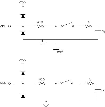 Figure 33. Equivalent Input Circuit for the Sampling Stage
The analog input full-scale range (FSR) is defined by the reference voltage of the ADC. The relationship between the FSR and the reference voltage can be determined by: FSR = VREF = AVDD.
8.3.3 ADC Transfer Function
The device output is in straight binary format. The device resolution can be computed by Equation 1:
where
- FSR = VREF = AVDD and
- N = 12
Figure 34 and Table 1 show the ideal transfer characteristics for the device.
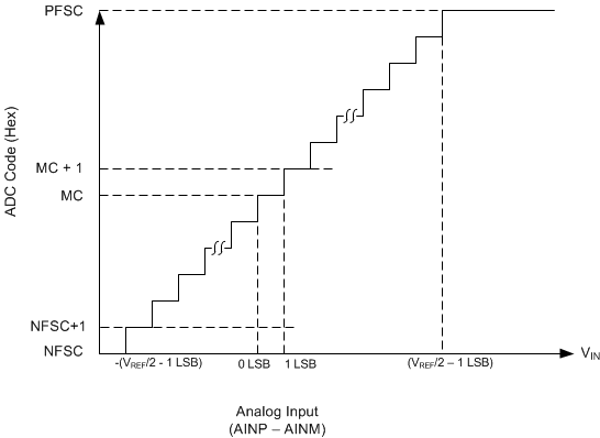 Figure 34. Ideal Transfer Characteristics
Table 1. Transfer Characteristics
| INPUT VOLTAGE (AINP-AINM) | CODE | DESCRIPTION | IDEAL OUTPUT CODE |
|---|---|---|---|
| ≤ –(VREF / 2 – 1 LSB) | NFSC | Negative full-scale code | 000 |
| –(VREF / 2 – 1 LSB) to –(VREF / 2 – 2 LSBs) |
NFSC + 1 | — | 001 |
| 0 to 1 LSB | MC | Mid code | 800 |
| 1 LSB to 2 LSBs | MC + 1 | — | 801 |
| ≥ VREF / 2 – 1 LSB | PFSC | Positive full-scale code | FFF |
8.3.4 Serial Interface
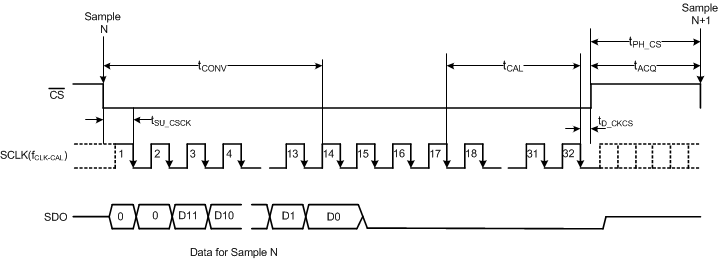
The device supports a simple, SPI-compatible interface to the external host. The CS signal defines one conversion and serial transfer frame. A frame starts with a CS falling edge and ends with a CS rising edge. The SDO pin outputs the ADC conversion results. Figure 35 shows a detailed timing diagram for the serial interface. A minimum delay of tSU_CSCK must elapse between the CS falling edge and the first SCLK falling edge. The device uses the clock provided on the SCLK pin for conversion and data transfer. The conversion result is available on the SDO pin with the first two bits set to 0, followed by 12 bits of the conversion result. The first zero is launched on the SDO pin on the CS falling edge. Subsequent bits (starting with another 0 followed by the conversion result) are launched on the SDO pin on subsequent SCLK falling edges. The SDO output remains low after 14 SCLKs. A CS rising edge ends the frame and brings the serial data bus to 3-state. For the acquisition of the next sample, a minimum time of tACQ must be provided after the conversion of the current sample is completed. For details on timing specifications, see the Timing Characteristics table.
The device initiates offset calibration on first CS falling edge after power-up and the SDO output remains low during the first serial transfer frame after power-up. For details, refer to the Offset Calibration section.
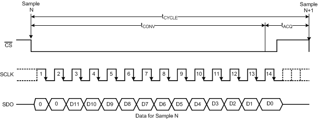 Figure 35. Serial Interface Timing Diagram
8.4 Device Functional Modes
8.4.1 Offset Calibration
The device includes a feature to calibrate its internal offset. The device initiates offset calibration on the first CS falling edge after power up and during offset calibration, the analog input pins (AINP and AINM) are disconnected from the sampling stage. After the first serial transfer frame, the device starts operating with either uncalibrated or calibrated offset, depending on the number of SCLKs provided in the first serial transfer frame. Offset calibration can also be initiated by the user during normal operation. Figure 36 shows the offset calibration process. The SDO output remains low during the first serial transfer frame.
The device includes an internal offset calibration register (OCR) that stores the offset calibration result. The OCR is an internal register and cannot be accessed by the user through the serial interface. The OCR is reset to zero on power-up. Therefore, TI recommends calibrating the offset on power-up to bring the offset within the specified limits. If there is a significant change in operating temperature or analog supply voltage, the offset can be recalibrated during normal operation.

8.4.1.1 Offset Calibration on Power-Up
The device starts offset calibration on the first CS falling edge after power-up and calibration completes if the CS pin remains low for at least 16 SCLKs after the first CS falling edge. The SDO output remains low during calibration. The minimum acquisition time must be provided after calibration for acquiring the first sample. If the device is not provided with at least 16 SCLKs during the first serial transfer frame after power-up, the OCR is not updated. Table 2 provides the timing parameters for offset calibration on power-up.
For subsequent samples, the device adjusts the conversion results with the value stored in the OCR. The conversion result adjusted with the value stored in OCR is provided by the device on the SDO output. Figure 37 shows the timing diagram for offset calibration on power-up.
Table 2. Offset Calibration on Power-Up
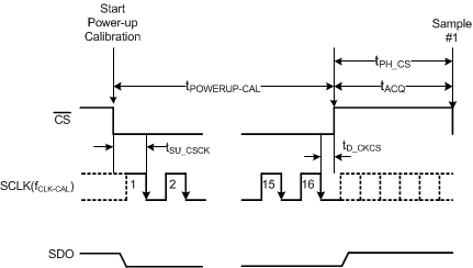 Figure 37. Offset Calibration on Power-Up Timing Diagram
8.4.1.2 Offset Calibration During Normal Operation
The offset can also be calibrated during normal device operation. Offset calibration can be done during normal device operation if at least 32 SCLKs are provided in one serial transfer frame. During the first 14 SCLKs, the device converts the sample acquired on the CS falling edge and provides data on the SDO output. The device initiates the offset calibration on the 17th SCLK falling edge and calibration is completed on the 32nd SCLK falling edge. The SDO output remains low after the 14th SCLK falling edge and SDO goes to 3-state after CS goes high. If the device is provided with less than 32 SCLKs during a serial transfer frame, the OCR is not updated. Table 3 provides the timing parameters for offset calibration during normal operation.
For subsequent samples, the device adjusts the conversion results with the value stored in OCR. The conversion result adjusted with the value stored in the OCR is provided by the device on the SDO output. Figure 38 shows the timing diagram for offset calibration during normal operation.
