SBAS891B November   2017  – September 2022 ADS7142-Q1

PRODUCTION DATA  

  1. Features
  2. Applications
  3. Description
  4. Revision History
  5. Pin Configuration and Functions
  6. Specifications
    1. 6.1  Absolute Maximum Ratings
    2. 6.2  ESD Ratings
    3. 6.3  Recommended Operating Conditions
    4. 6.4  Thermal Information
    5. 6.5  Electrical Characteristics: All Modes
    6. 6.6  Electrical Characteristics: Manual Mode
    7. 6.7  Electrical Characteristics: Autonomous Modes
    8. 6.8  Electrical Characteristics: High Precision Mode
    9. 6.9  Timing Requirements
    10. 6.10 Switching Characteristics
    11. 6.11 Timing Diagrams
    12. 6.12 Typical Characteristics: All Modes
    13. 6.13 Typical Characteristics: Manual Mode
    14. 6.14 Typical Characteristics: Autonomous Modes
    15. 6.15 Typical Characteristics: High-Precision Mode
  7. Detailed Description
    1. 7.1 Overview
    2. 7.2 Functional Block Diagram
    3. 7.3 Feature Description
      1. 7.3.1  Analog Input and Multiplexer
        1. 7.3.1.1 Two-Channel, Single-Ended Configuration
        2. 7.3.1.2 Single-Channel, Single-Ended Configuration With Remote Ground Sense
        3. 7.3.1.3 Single-Channel, Pseudo-Differential Configuration
      2. 7.3.2  Offset Calibration
      3. 7.3.3  Reference
      4. 7.3.4  ADC Transfer Function
      5. 7.3.5  Oscillator and Timing Control
      6. 7.3.6  I2C Address Selector
      7. 7.3.7  Data Buffer
        1. 7.3.7.1 Filling of the Data Buffer
        2. 7.3.7.2 Reading Data From the Data Buffer
      8. 7.3.8  Accumulator
      9. 7.3.9  Digital Window Comparator
      10. 7.3.10 I2C Protocol Features
        1. 7.3.10.1 General Call
        2. 7.3.10.2 General Call With Software Reset
        3. 7.3.10.3 General Call With Write Software Programmable Part of the Target Address
        4. 7.3.10.4 Configuring the ADC Into High-Speed I2C Mode
        5. 7.3.10.5 Bus Clear
    4. 7.4 Device Functional Modes
      1. 7.4.1 Device Power Up and Reset
      2. 7.4.2 Manual Mode
        1. 7.4.2.1 Manual Mode With CH0 Only
        2. 7.4.2.2 Manual Mode With AUTO Sequence
      3. 7.4.3 Autonomous Modes
        1. 7.4.3.1 Autonomous Mode With Threshold Monitoring and Diagnostics
          1. 7.4.3.1.1 Autonomous Mode With Pre-ALERT Data
          2. 7.4.3.1.2 Autonomous Mode With Post-ALERT Data
        2. 7.4.3.2 Autonomous Mode With Burst Data
          1. 7.4.3.2.1 Autonomous Mode With Start Burst
          2. 7.4.3.2.2 Autonomous Mode With Stop Burst
      4. 7.4.4 High-Precision Mode
    5. 7.5 Programming
      1. 7.5.1 Reading Registers
        1. 7.5.1.1 Single Register Read
        2. 7.5.1.2 Reading a Continuous Block of Registers
      2. 7.5.2 Writing Registers
        1. 7.5.2.1 Single Register Write
        2. 7.5.2.2 Writing a Continuous Block of Registers
        3. 7.5.2.3 Set Bit
        4. 7.5.2.4 Clear Bit
    6. 7.6 Register Map
      1. 7.6.1 Page1 Registers
  8. Application and Implementation
    1. 8.1 Application Information
    2. 8.2 Typical Applications
      1. 8.2.1 ADS7142-Q1 as a Programmable Comparator With False Trigger Prevention and Diagnostics
        1. 8.2.1.1 Design Requirements
        2. 8.2.1.2 Detailed Design Procedure
          1. 8.2.1.2.1 Programmable Thresholds and Hysteresis
          2. 8.2.1.2.2 False Trigger Prevention With an Event Counter
          3. 8.2.1.2.3 Fault Diagnostics With the Data Buffer
        3. 8.2.1.3 Application Curves
      2. 8.2.2 Voltage and Temperature Monitoring in Remote Camera Modules Using the ADS7142-Q1
        1. 8.2.2.1 Design Requirements
    3. 8.3 Power Supply Recommendations
      1. 8.3.1 AVDD and DVDD Supply Recommendations
    4. 8.4 Layout
      1. 8.4.1 Layout Guidelines
      2. 8.4.2 Layout Example
  9. Device and Documentation Support
    1. 9.1 Electrostatic Discharge Caution
    2. 9.2 Glossary
    3. 9.3 Trademarks
    4. 9.4 Receiving Notification of Documentation Updates
    5. 9.5 Support Resources
  10. 10Mechanical, Packaging, and Orderable Information

Package Options

Mechanical Data (Package|Pins)
Thermal pad, mechanical data (Package|Pins)
Orderable Information

Manual Mode With AUTO Sequence

Set the OPMODE_SEL register to 100b or 101b for manual mode with AUTO sequence. The host must set the SEQ_START bit in the START_SEQUENCE register and provide the device address and read bit to start the conversions. To continue with conversions and reading data, the host must provide continuous SCL (Figure 7-13). In this mode, the SEQ_ABORT bit in the ABORT_SEQUENCE register must be set to abort the operation. Then the device operation mode can be changed to another operation mode. In this mode, a register read aborts the AUTO sequence.

In manual mode, the device always uses the high-speed oscillator and the nCLK parameter has no effect. The maximum scan rate is given by Equation 7:

Equation 7. GUID-EDA8DE26-D611-4420-BD63-68E51C78B40E-low.gif
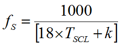
  • fs = Maximum sampling speed in kSPS
  • TSCL= Time period of SCL clock (in µs)
  • if TSCL-LOW (low period of SCL) < 1.8.µs, k = (1.8 – TSCL-LOW) and the device stretches clock in manual mode; not applicable for standard I2C mode (100 kHz)
  • if TSCL-LOW (low period of SCL) ≥ 1.8.µs, k = 0, and the device does not stretch clock in manual mode
GUID-D57DA115-83DF-4C6D-85E8-0C857B7DAAEE-low.gif
For setting the operation mode to manual mode, see Figure 7-11.
Select manual mode with AUTO sequence in the OPMODE_SEL register. Select channels in the AUTO_SEQ_CHEN register.
Set the SEQ_START bit in the START_SEQUENCE register.
See Figure 7-13.
Set the SEQ_ABORT bit in the ABORT_SEQUENCE register.
Select another operation mode in the OPMODE_SEL register.
For reading and writing registers, see the Section 7.5 section.
Figure 7-12 Device Operation in Manual Mode

Data can be read from the device by providing a device address and read bit followed by continuous SCL, as shown in Figure 7-13.

GUID-707C3418-DAEB-4BD8-997F-9AFDD349A4C7-low.gif
See Equation 7 for sampling speed in manual mode.
If the device scans both channels in AUTO sequence, the first data (for sample A) is from channel 0 and the second data (for sample A +1) is from channel 1.
Figure 7-13 Starting Conversion and Reading Data in Manual Mode