SBAS584B October 2013 – August 2014 ADS7253 , ADS7853 , ADS8353
PRODUCTION DATA.
- 1 Features
- 2 Applications
- 3 Description
- 4 Revision History
- 5 Device Comparison Table
- 6 Pin Configurations and Functions
-
7 Specifications
- 7.1 Absolute Maximum Ratings
- 7.2 Handling Ratings
- 7.3 Recommended Operating Conditions
- 7.4 Thermal Information
- 7.5 Electrical Characteristics: ADS8353
- 7.6 Electrical Characteristics: ADS7853
- 7.7 Electrical Characteristics: ADS7253
- 7.8 Electrical Characteristics: All Devices
- 7.9 Timing Requirements: Interface Mode
- 7.10 Timing Characteristics: Serial Interface
- 7.11 Typical Characteristics: ADS8353
- 7.12 Typical Characteristics: ADS7853
- 7.13 Typical Characteristics: ADS7253
- 7.14 Typical Characteristics: Common to ADS8353, ADS7853, and ADS7253
-
8 Detailed Description
- 8.1 Overview
- 8.2 Functional Block Diagram
- 8.3 Feature Description
- 8.4 Device Functional Modes
- 8.5 Register Maps and Serial Interface
- 9 Application and Implementation
- 10Power-Supply Recommendations
- 11Layout
- 12Device and Documentation Support
- 13Mechanical, Packaging, and Orderable Information
Package Options
Mechanical Data (Package|Pins)
Thermal pad, mechanical data (Package|Pins)
- RTE|16
Orderable Information
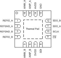
6 Pin Configurations and Functions
RTE Package
WQFN-16
(Top View)
PW Package
TSSOP-16
(Top View)
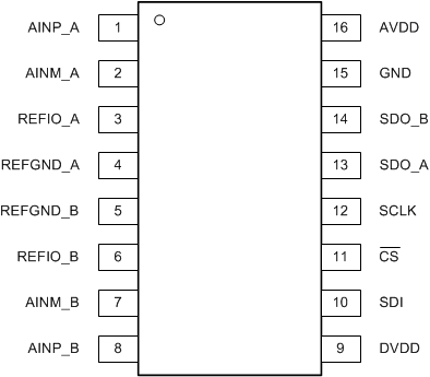
Pin Functions
| PIN | I/O | DESCRIPTION | ||
|---|---|---|---|---|
| NAME | NO. | |||
| TSSOP | WQFN | |||
| AINM_A | 2 | 16 | Analog input | Negative analog input, channel A |
| AINM_B | 7 | 5 | Analog input | Negative analog input, channel B |
| AINP_A | 1 | 15 | Analog input | Positive analog input, channel A |
| AINP_B | 8 | 6 | Analog input | Positive analog input, channel B |
| AVDD | 16 | 14 | Supply | Supply voltage for ADC operation |
| CS | 11 | 9 | Digital input | Chip-select signal; active low |
| DVDD | 9 | 7 | Digital I/O supply | Digital I/O supply |
| GND | 15 | 13 | Supply | Digital ground |
| REFGND_A | 4 | 2 | Supply | Reference ground potential A |
| REFGND_B | 5 | 3 | Supply | Reference ground potential B |
| REFIO_A | 3 | 1 | Analog input/output | Reference voltage input/output, channel A |
| REFIO_B | 6 | 4 | Analog input/output | Reference voltage input/output, channel B |
| SCLK | 12 | 10 | Digital input | Clock for serial communication |
| SDI | 10 | 8 | Digital input | Data input for serial communication |
| SDO_A | 13 | 11 | Digital output | Data output for serial communication, channel A and channel B |
| SDO_B | 14 | 12 | Digital output | Data output for serial communication, channel B |
| Thermal pad | — | Thermal pad | Supply | Exposed thermal pad (only for WQFN). TI recommends connecting this pin to the printed circuit board (PCB) ground. |