SBAS482C January 2010 – September 2017 ADS7924
PRODUCTION DATA.
- 1 Features
- 2 Applications
- 3 Description
- 4 Revision History
- 5 Pin Configuration and Functions
- 6 Specifications
- 7 Detailed Description
-
8 Application and Implementation
- 8.1
Application Information
- 8.1.1 Using an Operational Amplifier Between Multiplexer Output and ADC Input
- 8.1.2 Using an Operational Amplifier and RC Filter Between Multiplexer Output and ADC Input
- 8.1.3 Using an RC Filter Between Multiplexer Output and ADC Input
- 8.1.4 Operational Amplifier With Filter and Gain Option Between Multiplexer Output and ADC Input
- 8.1.5 Driving an RC Filter With an Operational Amplifier Between Multiplexer Output and ADC Input
- 8.1.6 Average Power Consumption
- 8.2 Typical Application
- 8.1
Application Information
- 9 Power Supply Recommendations
- 10Layout
- 11Device and Documentation Support
- 12Mechanical, Packaging, and Orderable Information
Package Options
Mechanical Data (Package|Pins)
- RTE|16
Thermal pad, mechanical data (Package|Pins)
- RTE|16
Orderable Information
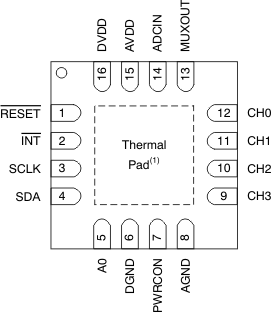
5 Pin Configuration and Functions
RTE Package
16-Pin WQFN
Top View

1. Connect to AGND.
Pin Functions
| PIN | I/O | DESCRIPTION | |
|---|---|---|---|
| NO. | NAME | ||
| 1 | RESET | Digital input | External reset, active low |
| 2 | INT | Digital output | Interrupt pin, active low; generated when input voltage is beyond programmed threshold |
| 3 | SCLK | Digital input | Serial clock input |
| 4 | SDA | Digital input/output | Serial data |
| 5 | A0 | Digital input | I2C address selection |
| 6 | DGND | Digital | Digital ground |
| 7 | PWRCON | Digital output | Power control pin to control shutdown/power-up of external operational amplifier |
| 8 | AGND | Analog | Analog ground |
| 9 | CH3 | Analog input | Input channel 3 |
| 10 | CH2 | Analog input | Input channel 2 |
| 11 | CH1 | Analog input | Input channel 1 |
| 12 | CH0 | Analog input | Input channel 0 |
| 13 | MUXOUT | Analog output | Multiplexer output |
| 14 | ADCIN | Analog input | ADC input |
| 15 | AVDD | Analog | Analog supply |
| 16 | DVDD | Digital | Digital supply |