SBAS482C January 2010 – September 2017 ADS7924
PRODUCTION DATA.
- 1 Features
- 2 Applications
- 3 Description
- 4 Revision History
- 5 Pin Configuration and Functions
- 6 Specifications
- 7 Detailed Description
-
8 Application and Implementation
- 8.1
Application Information
- 8.1.1 Using an Operational Amplifier Between Multiplexer Output and ADC Input
- 8.1.2 Using an Operational Amplifier and RC Filter Between Multiplexer Output and ADC Input
- 8.1.3 Using an RC Filter Between Multiplexer Output and ADC Input
- 8.1.4 Operational Amplifier With Filter and Gain Option Between Multiplexer Output and ADC Input
- 8.1.5 Driving an RC Filter With an Operational Amplifier Between Multiplexer Output and ADC Input
- 8.1.6 Average Power Consumption
- 8.2 Typical Application
- 8.1
Application Information
- 9 Power Supply Recommendations
- 10Layout
- 11Device and Documentation Support
- 12Mechanical, Packaging, and Orderable Information
Package Options
Mechanical Data (Package|Pins)
- RTE|16
Thermal pad, mechanical data (Package|Pins)
- RTE|16
Orderable Information
6 Specifications
6.1 Absolute Maximum Ratings
Over operating free-air temperature range, unless otherwise noted.(1)
(1) Stresses beyond those listed under Absolute Maximum Ratings may cause permanent damage to the device. These are stress ratings only, which do not imply functional operation of the device at these or any other conditions beyond those indicated under Recommended Operating Conditions. Exposure to absolute-maximum-rated conditions for extended periods may affect device reliability.
6.2 ESD Ratings
| VALUE | UNIT | |||
|---|---|---|---|---|
| V(ESD) | Electrostatic discharge | Human-body model (HBM), per ANSI/ESDA/JEDEC JS-001(1) | ±2000 | V |
| Charged-device model (CDM), per JEDEC specification JESD22-C101(2) | ±750 | |||
(1) JEDEC document JEP155 states that 500-V HBM allows safe manufacturing with a standard ESD control process.
(2) JEDEC document JEP157 states that 250-V CDM allows safe manufacturing with a standard ESD control process.
6.3 Recommended Operating Conditions
over operating free-air temperature range (unless otherwise noted)| MIN | NOM | MAX | UNIT | ||
|---|---|---|---|---|---|
| AVDD | Analog Supply Voltage | 2.2 | 5.5 | V | |
| DVDD | Digital Supply Voltage | 1.65 | AVDD | V | |
6.4 Thermal Information
| THERMAL METRIC(1) | ADS7924 | UNIT | |
|---|---|---|---|
| RTE (WQFN) | |||
| 16 PINS | |||
| RθJA | Junction-to-ambient thermal resistance | 48.1 | °C/W |
| RθJC(top) | Junction-to-case(top) thermal resistance | 47.3 | °C/W |
| RθJB | Junction-to-board thermal resistance | 60.8 | °C/W |
| ψJT | Junction-to-top characterization parameter | 0.3 | °C/W |
| ψJB | Junction-to-board characterization parameter | 14.1 | °C/W |
| RθJC(bot) | Junction-to-case(bottom) thermal resistance | 0.4 | °C/W |
(1) For more information about traditional and new thermal metrics, see the Semiconductor and IC Package Thermal Metrics application report.
6.5 Electrical Characteristics
Minimum and maximum specifications are at TA = –40°C to 85°C, 1.65 V < DVDD < 5.5 V, and 2.2 V < AVDD < 5.5 V. Typical specifications are at TA = 25°C, AVDD = 5 V, and DVDD = 5 V, unless otherwise noted.| PARAMETER | TEST CONDITIONS | MIN | TYP | MAX | UNIT | ||
|---|---|---|---|---|---|---|---|
| ANALOG INPUT | |||||||
| Full-scale input span | (CHX – AGND) | 0 | AVDD | V | |||
| Input capacitance(1) | 4 | 10 | pF | ||||
| ADC sampling capacitance | 15 | pF | |||||
| MUX resistance | 60 | Ω | |||||
| Input channel crosstalk | 85 | dB | |||||
| SYSTEM PERFORMANCE | |||||||
| Resolution | 12 | Bits | |||||
| No missing codes | 12 | Bits | |||||
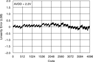
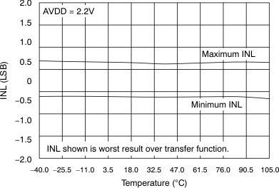
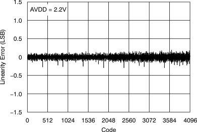
| Integral linearity | –1.5 | ±0.5 | 1.5 | LSBs | |||
| Differential linearity | –1 | ±0.6 | 1.5 | LSBs | |||
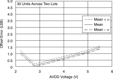
| Offset error | –5 | 5 | LSBs | ||||
| Offset error drift | 0.01 | LSB/°C | |||||
| Gain error | –0.2% | –0.01% | 0.2% | ||||
| Gain error drift | 0.6 | ppm/°C | |||||
| Noise (rms) | 0.125 | LSB | |||||
| SAMPLING DYNAMICS | |||||||
| Monitoring time/channel(3) | 10 | µs | |||||
| CLOCK | |||||||
| Internal clock frequency variation | ±20% | ||||||
| DIGITAL INPUT/OUTPUT | |||||||
| Logic family | CMOS | ||||||
| Logic level: | |||||||
| VIH (SDA, SCL, A0, RESET) | 0.8 DVDD | DVDD + 0.3 | V | ||||
| VIL (SDA, SCL, A0, RESET) | DGND – 0.3 | 0.4 | V | ||||
| Input current | II | VI = DVDD or DGND | –10 | 10 | μA | ||
| VOH (PWRCON, INT) | IOH = 100 μA, INT pin | 0.8 DVDD | DVDD | V | |||
| IOH = 100 µA, PWRCON pin | 0.8 AVDD | AVDD | V | ||||
| VOL (PWRCON, INT, SDA) | IOL = 100 μA | DGND | 0.4 | V | |||
| Low-level output current | IOL | SDA pin, VOL = 0.6 V | 3 | mA | |||
| Load capacitance | CB | SDA pin | 400 | pF | |||
| Data format | Straight binary | ||||||
| POWER-SUPPLY REQUIREMENTS | |||||||
| Power-supply voltage: | |||||||
| DVDD(2) | 1.65 | 5.5 | V | ||||
| AVDD | 2.2 | 5.5 | V | ||||
| IAVDD(4) | tCYCLE = 2.5 ms, AVDD = 2.2 V | 5 | 8 | μA | |||
| IPWRD, power-down current | <1 | μA | |||||
| TEMPERATURE RANGE | |||||||
| Specified performance | –40 | 85 | °C | ||||
(1) CH0 to CH3 input pin capacitance.
(2) DVDD cannot exceed AVDD.
(3) Rate at which channels can be scanned. This is the minimum acquisition time (6 µs) and conversion time (4 µs).
6.6 I2C Timing Requirements
| MIN | MAX | UNIT | ||
|---|---|---|---|---|
| fSCL | SCL operating frequency | 0 | 0.4 | MHz |
| tBUF | Bus free time between START and STOP condition | 1.3 | μs | |
| tHDSTA | Hold time after repeated START condition. After this period, the first clock is generated. |
600 | ns | |
| tSUSTA | Repeated START condition setup time | 600 | ns | |
| tSUSTO | Stop condition setup time | 600 | ns | |
| tHDDAT | Data hold time | 0 | ns | |
| tSUDAT | Data setup time | 100 | ns | |
| tLOW | SCL clock low period | 1300 | ns | |
| tHIGH | SCL clock high period | 600 | ns | |
| tF | Clock/data fall time | 300 | ns | |
| tR | Clock/data rise time | 300 | ns | |
| tVDDAT | Data valid time | 0.9 | μs | |
| tVDACK | Data valid acknowledge time | 0.9 | μs | |
| tSP | Pulse width of spike that must be suppressed by the input filter | 0 | 50 | ns |

NOTE: S = Start, Sr = Repeated Start, and P = Stop.
Figure 1. I2C Timing Diagram
6.7 Typical Characteristics
At TA = 25°C, unless otherwise noted.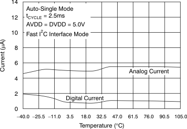
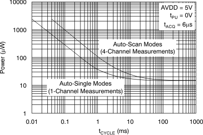
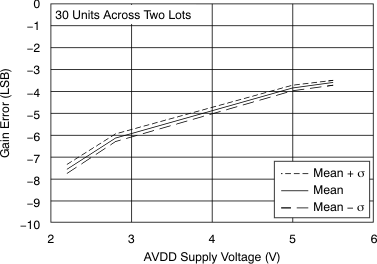
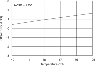
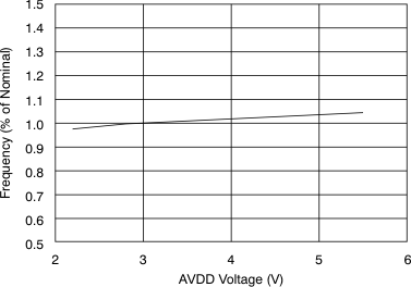
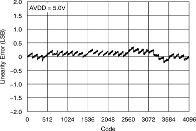
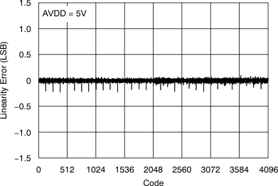
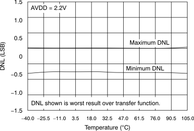
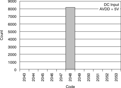
| At code center |
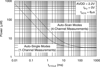
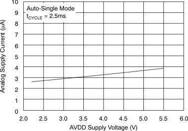
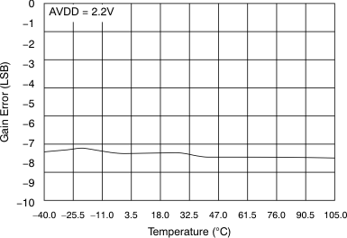
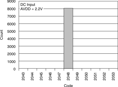
| At code center |
1. At code center.