SBAS931B January   2019  – July 2022 ADS8353-Q1

PRODUCTION DATA  

  1. 1Features
  2. 2Applications
  3. 3Description
  4. 4Revision History
  5. 5Pin Configuration and Functions
  6. 6Specifications
    1. 6.1 Absolute Maximum Ratings
    2. 6.2 ESD Ratings
    3. 6.3 Thermal Information
    4. 6.4 Recommended Operating Conditions
    5. 6.5 Electrical Characteristics
    6. 6.6 Timing Requirements
    7. 6.7 Switching Characteristics
    8. 6.8 Timing Diagram
    9. 6.9 Typical Characteristics
  7. 7Detailed Description
    1. 7.1 Overview
    2. 7.2 Functional Block Diagram
    3. 7.3 Feature Description
      1. 7.3.1 Reference
      2. 7.3.2 Analog Inputs
        1. 7.3.2.1 Analog Input: Full-Scale Range Selection
        2. 7.3.2.2 Analog Input: Single-Ended and Pseudo-Differential Configurations
      3. 7.3.3 Transfer Function
    4. 7.4 Device Functional Modes
    5. 7.5 Programming
      1. 7.5.1 Serial Interface
      2. 7.5.2 Write to User-Programmable Registers
      3. 7.5.3 Data Read Operation
        1. 7.5.3.1 Reading User-Programmable Registers
        2. 7.5.3.2 Conversion Data Read
          1. 7.5.3.2.1 32-CLK, Dual-SDO Mode (CFR.B11 = 0, CFR.B10 = 0, Default)
          2. 7.5.3.2.2 32-CLK, Single-SDO Mode (CFR.B11 = 0, CFR.B10 = 1)
      4. 7.5.4 Low-Power Modes
        1. 7.5.4.1 STANDBY Mode
        2. 7.5.4.2 Software Power-Down (SPD) Mode
      5. 7.5.5 Frame Abort, Reconversion, or Short-Cycling
    6. 7.6 Register Maps
      1. 7.6.1 ADS8353-Q1 Registers
  8. 8Application and Implementation
    1. 8.1 Application Information
      1. 8.1.1 Input Amplifier Selection
      2. 8.1.2 Charge Kickback Filter
    2. 8.2 Typical Application
      1. 8.2.1 Design Requirements
      2. 8.2.2 Detailed Design Procedure
      3. 8.2.3 Application Curve
    3. 8.3 Power Supply Recommendations
    4. 8.4 Layout
      1. 8.4.1 Layout Guidelines
      2. 8.4.2 Layout Example
  9. 9Device and Documentation Support
    1. 9.1 Device Support
      1. 9.1.1 Development Support
    2. 9.2 Documentation Support
      1. 9.2.1 Related Documentation
    3. 9.3 Receiving Notification of Documentation Updates
    4. 9.4 Support Resources
    5. 9.5 Trademarks
    6. 9.6 Electrostatic Discharge Caution
    7. 9.7 Glossary
      1.      Mechanical, Packaging, and Orderable Information

Package Options

Mechanical Data (Package|Pins)
Thermal pad, mechanical data (Package|Pins)
Orderable Information

Reference

The device has two simultaneous sampling ADCs (ADC_A and ADC_B). ADC_A and ADC_B operate with reference voltages present on the REFIO_A and REFIO_B pins, respectively. Decouple the REFIO_A and REFIO_B pins with the REFGND_A and REFGND_B pins, respectively, with 10-µF decoupling capacitors.

Figure 7-1 shows that the device supports operation either with an internal or external reference source. The reference voltage source is determined by setting bit 6 of the configuration register (CFR.B6). This bit is common to ADC_A and ADC_B.
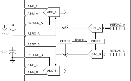
GUID-C99CEC2E-FCFE-4D85-88A7-DE5891F921F1-low.gifFigure 7-1 Reference Configurations and Connections

When CFR.B6 is 0, the device shuts down the internal reference source (INTREF) and ADC_A and ADC_B operate on external reference voltages provided by the user on the REFIO_A and REFIO_B pins, respectively.

When CFR.B6 is 1, the device operates with the internal reference source (INTREF) connected to REFIO_A and REFIO_B via DAC_A and DAC_B, respectively. In this configuration, VREF_A and VREF_B can be changed independently by writing to the respective user-programmable registers, REFDAC_A and REFDAC_B, respectively. See the Section 7.6 section for more details.