SBAS931B January   2019  – July 2022 ADS8353-Q1

PRODUCTION DATA  

  1. 1Features
  2. 2Applications
  3. 3Description
  4. 4Revision History
  5. 5Pin Configuration and Functions
  6. 6Specifications
    1. 6.1 Absolute Maximum Ratings
    2. 6.2 ESD Ratings
    3. 6.3 Thermal Information
    4. 6.4 Recommended Operating Conditions
    5. 6.5 Electrical Characteristics
    6. 6.6 Timing Requirements
    7. 6.7 Switching Characteristics
    8. 6.8 Timing Diagram
    9. 6.9 Typical Characteristics
  7. 7Detailed Description
    1. 7.1 Overview
    2. 7.2 Functional Block Diagram
    3. 7.3 Feature Description
      1. 7.3.1 Reference
      2. 7.3.2 Analog Inputs
        1. 7.3.2.1 Analog Input: Full-Scale Range Selection
        2. 7.3.2.2 Analog Input: Single-Ended and Pseudo-Differential Configurations
      3. 7.3.3 Transfer Function
    4. 7.4 Device Functional Modes
    5. 7.5 Programming
      1. 7.5.1 Serial Interface
      2. 7.5.2 Write to User-Programmable Registers
      3. 7.5.3 Data Read Operation
        1. 7.5.3.1 Reading User-Programmable Registers
        2. 7.5.3.2 Conversion Data Read
          1. 7.5.3.2.1 32-CLK, Dual-SDO Mode (CFR.B11 = 0, CFR.B10 = 0, Default)
          2. 7.5.3.2.2 32-CLK, Single-SDO Mode (CFR.B11 = 0, CFR.B10 = 1)
      4. 7.5.4 Low-Power Modes
        1. 7.5.4.1 STANDBY Mode
        2. 7.5.4.2 Software Power-Down (SPD) Mode
      5. 7.5.5 Frame Abort, Reconversion, or Short-Cycling
    6. 7.6 Register Maps
      1. 7.6.1 ADS8353-Q1 Registers
  8. 8Application and Implementation
    1. 8.1 Application Information
      1. 8.1.1 Input Amplifier Selection
      2. 8.1.2 Charge Kickback Filter
    2. 8.2 Typical Application
      1. 8.2.1 Design Requirements
      2. 8.2.2 Detailed Design Procedure
      3. 8.2.3 Application Curve
    3. 8.3 Power Supply Recommendations
    4. 8.4 Layout
      1. 8.4.1 Layout Guidelines
      2. 8.4.2 Layout Example
  9. 9Device and Documentation Support
    1. 9.1 Device Support
      1. 9.1.1 Development Support
    2. 9.2 Documentation Support
      1. 9.2.1 Related Documentation
    3. 9.3 Receiving Notification of Documentation Updates
    4. 9.4 Support Resources
    5. 9.5 Trademarks
    6. 9.6 Electrostatic Discharge Caution
    7. 9.7 Glossary
      1.      Mechanical, Packaging, and Orderable Information

Package Options

Mechanical Data (Package|Pins)
Thermal pad, mechanical data (Package|Pins)
Orderable Information

Frame Abort, Reconversion, or Short-Cycling

As shown in Figure 7-12, the minimum number of SCLK falling edges (N) that must be provided between the beginning and end of the frame depends on the serial interface mode. The SCLK falling edges (N) program the device and retrieve the conversion result. If CS is brought high before the expected number of SCLK falling edges are provided, the current frame is aborted and the device starts sampling the new analog input signal.

If frame (F) is aborted, then the register write operation attempted in frame (F) is considered invalid and the internal registers are not updated. The device continues to have the same configuration in frame (F+1) from frame (F).

The output data bits latched before the CS rising edge are still valid data that correspond to sample N.
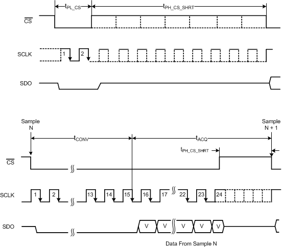
GUID-D040385E-839D-467F-8C0C-4046FF98801F-low.gifFigure 7-12 Frame Abort, Reconversion, or Short-Cycling Feature

See the Section 6.6 table for timing specifications for this operating mode.