SBAS556B October 2013 – August 2014 ADS7254 , ADS7854 , ADS8354
PRODUCTION DATA.
- 1 Features
- 2 Applications
- 3 Description
- 4 Revision History
- 5 Device Comparison Table
- 6 Pin Configurations and Functions
-
7 Specifications
- 7.1 Absolute Maximum Ratings
- 7.2 Handling Ratings
- 7.3 Recommended Operating Conditions
- 7.4 Thermal Information
- 7.5 Electrical Characteristics: ADS8354
- 7.6 Electrical Characteristics: ADS7854
- 7.7 Electrical Characteristics: ADS7254
- 7.8 Electrical Characteristics: All Devices
- 7.9 Timing Requirements: Interface Mode
- 7.10 Timing Characteristics: Serial Interface
- 7.11 Typical Characteristics: ADS8354
- 7.12 Typical Characteristics: ADS7854
- 7.13 Typical Characteristics: ADS7254
- 7.14 Typical Characteristics: Common to ADS8354, ADS7854, and ADS7254
-
8 Detailed Description
- 8.1 Overview
- 8.2 Functional Block Diagram
- 8.3 Feature Description
- 8.4 Device Functional Modes
- 8.5 Register Maps and Serial Interface
- 9 Application and Implementation
- 10Power-Supply Recommendations
- 11Layout
- 12Device and Documentation Support
- 13Mechanical, Packaging, and Orderable Information
Package Options
Mechanical Data (Package|Pins)
Thermal pad, mechanical data (Package|Pins)
- RTE|16
Orderable Information
10 Power-Supply Recommendations
The devices have two separate power supplies: AVDD and DVDD. The device operates on AVDD; DVDD is used for the interface circuits. AVDD and DVDD can be independently set to any value within the permissible ranges.
When using the device with ±2 × VREF input range (CFR.B9 = 1), the AVDD supply voltage value defines the permissible voltage swing on the analog input pins. To avoid saturation of output codes, and to use the full dynamic range on the analog input pins, AVDD must be set as shown in Equation 11, Equation 12, and Equation 13:
Decouple the AVDD and DVDD pins with the GND pin using individual 10-µF decoupling capacitors, as shown in Figure 115.
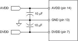 Figure 115. Power-Supply Decoupling