SBAS492 July 2015 ADS8664 , ADS8668
PRODUCTION DATA.
- 1 Features
- 2 Applications
- 3 Description
- 4 Revision History
- 5 Device Comparison Table
- 6 Pin Configuration and Functions
- 7 Specifications
-
8 Detailed Description
- 8.1 Overview
- 8.2 Functional Block Diagram
- 8.3
Feature Description
- 8.3.1 Analog Inputs
- 8.3.2 Analog Input Impedance
- 8.3.3 Input Overvoltage Protection Circuit
- 8.3.4 Programmable Gain Amplifier (PGA)
- 8.3.5 Second-Order, Low-Pass Filter (LPF)
- 8.3.6 ADC Driver
- 8.3.7 Multiplexer (MUX)
- 8.3.8 Reference
- 8.3.9 Auxiliary Channel
- 8.3.10 ADC Transfer Function
- 8.3.11 Alarm Feature
- 8.4
Device Functional Modes
- 8.4.1 Device Interface
- 8.4.2
Device Modes
- 8.4.2.1 Continued Operation in the Selected Mode (NO_OP)
- 8.4.2.2 Frame Abort Condition (FRAME_ABORT)
- 8.4.2.3 STANDBY Mode (STDBY)
- 8.4.2.4 Power-Down Mode (PWR_DN)
- 8.4.2.5 Auto Channel Enable with Reset (AUTO_RST)
- 8.4.2.6 Manual Channel n Select (MAN_Ch_n)
- 8.4.2.7 Channel Sequencing Modes
- 8.4.2.8 Reset Program Registers (RST)
- 8.5
Register Maps
- 8.5.1 Command Register Description
- 8.5.2
Program Register Description
- 8.5.2.1 Program Register Read/Write Operation
- 8.5.2.2 Program Register Map
- 8.5.2.3
Program Register Descriptions
- 8.5.2.3.1 Auto-Scan Sequencing Control Registers
- 8.5.2.3.2 Device Features Selection Control Register (address = 03h)
- 8.5.2.3.3 Range Select Registers (addresses 05h-0Ch)
- 8.5.2.3.4 Alarm Flag Registers (Read-Only)
- 8.5.2.3.5 Alarm Threshold Setting Registers
- 8.5.2.3.6 Command Read-Back Register (address = 3Fh)
- 9 Application and Implementation
- 10Power-Supply Recommendations
- 11Layout
- 12Device and Documentation Support
- 13Mechanical, Packaging, and Orderable Information
Package Options
Mechanical Data (Package|Pins)
- DBT|38
Thermal pad, mechanical data (Package|Pins)
Orderable Information
11 Layout
11.1 Layout Guidelines
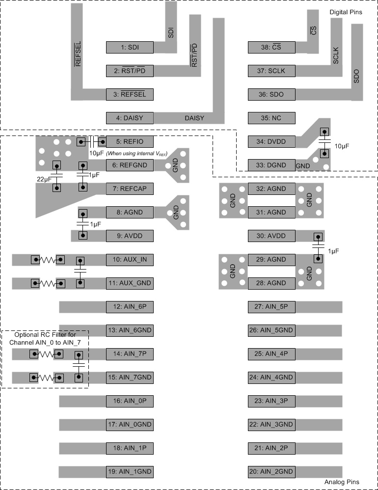
Figure 128 illustrates a PCB layout example for the ADS8664 and ADS8668.
- Partition the PCB into analog and digital sections. Care must be taken to ensure that the analog signals are kept away from the digital lines. This layout helps keep the analog input and reference input signals away from the digital noise. In this layout example, the analog input and reference signals are routed on the lower side of the board and the digital connections are routed on the top side of the board.
- Using a single dedicated ground plane is strongly encouraged.
- Power sources to the ADS8664 and ADS8668 must be clean and well-bypassed. TI recommends using a
1-μF, X7R-grade, 0603-size ceramic capacitor with at least a 10-V rating in close proximity to the analog (AVDD) supply pins. For decoupling the digital (DVDD) supply pin, a 10-μF, X7R-grade, 0805-size ceramic capacitor with at least a 10-V rating is recommended. Placing vias between the AVDD, DVDD pins and the bypass capacitors must be avoided. All ground pins must be connected to the ground plane using short, low impedance paths. - There are two decoupling capacitors used for the REFCAP pin. The first is a small, 1-μF, X7R-grade, 0603-size ceramic capacitor placed close to the device pins for decoupling the high-frequency signals and the second is a 22-µF, X7R-grade, 1210-size ceramic capacitor to provide the charge required by the reference circuit of the device. Both of these capacitors must be directly connected to the device pins without any vias between the pins and capacitors.
- The REFIO pin also must be decoupled with a 10-µF ceramic capacitor, if the internal reference of the device is used. The capacitor must be placed close to the device pins.
- For the auxiliary channel, the fly-wheel RC filter components must be placed close to the device. Among ceramic surface-mount capacitors, COG (NPO) ceramic capacitors provide the best capacitance precision. The type of dielectric used in COG (NPO) ceramic capacitors provides the most stable electrical properties over voltage, frequency, and temperature changes.
11.2 Layout Example
 Figure 128. Board Layout for the ADS8664 and ADS8668