SBAS572B May   2013  – March 2019 ADS8864

PRODUCTION DATA.  

  1. Features
  2. Applications
  3. Description
    1.     Device Images
      1.      No Separate LDO Required for the ADC Supply
  4. Revision History
  5. Device Comparison Table
  6. Pin Configuration and Functions
    1.     Pin Functions
  7. Specifications
    1. 7.1 Absolute Maximum Ratings
    2. 7.2 ESD Ratings
    3. 7.3 Recommended Operating Conditions
    4. 7.4 Thermal Information
    5. 7.5 Electrical Characteristics
    6. 7.6 Timing Requirements: 3-Wire Operation
    7. 7.7 Timing Requirements: 4-Wire Operation
    8. 7.8 Timing Requirements: Daisy-Chain
    9. 7.9 Typical Characteristics
  8. Parameter Measurement Information
    1. 8.1 Equivalent Circuits
  9. Detailed Description
    1. 9.1 Overview
    2. 9.2 Functional Block Diagram
    3. 9.3 Feature Description
      1. 9.3.1 Analog Input
      2. 9.3.2 Reference
      3. 9.3.3 Clock
      4. 9.3.4 ADC Transfer Function
    4. 9.4 Device Functional Modes
      1. 9.4.1 CS Mode
        1. 9.4.1.1 3-Wire CS Mode Without a Busy Indicator
        2. 9.4.1.2 3-Wire CS Mode With a Busy Indicator
        3. 9.4.1.3 4-Wire CS Mode Without a Busy Indicator
        4. 9.4.1.4 4-Wire CS Mode With a Busy Indicator
      2. 9.4.2 Daisy-Chain Mode
        1. 9.4.2.1 Daisy-Chain Mode Without a Busy Indicator
        2. 9.4.2.2 Daisy-Chain Mode With a Busy Indicator
  10. 10Application and Implementation
    1. 10.1 Application Information
      1. 10.1.1 ADC Reference Driver
      2. 10.1.2 ADC Input Driver
        1. 10.1.2.1 Input Amplifier Selection
        2. 10.1.2.2 Charge-Kickback Filter
    2. 10.2 Typical Applications
      1. 10.2.1 DAQ Circuit for a 2.5-µs, Full-Scale Step Response
        1. 10.2.1.1 Design Requirements
        2. 10.2.1.2 Detailed Design Procedure
      2. 10.2.2 DAQ Circuit for Lowest Distortion and Noise Performance at 400 kSPS
        1. 10.2.2.1 Design Requirements
        2. 10.2.2.2 Detailed Design Procedure
      3. 10.2.3 Ultralow-Power DAQ Circuit at 10 kSPS
        1. 10.2.3.1 Design Requirements
        2. 10.2.3.2 Detailed Design Procedure
  11. 11Power Supply Recommendations
    1. 11.1 Power-Supply Decoupling
    2. 11.2 Power Saving
  12. 12Layout
    1. 12.1 Layout Guidelines
    2. 12.2 Layout Example
  13. 13Device and Documentation Support
    1. 13.1 Documentation Support
      1. 13.1.1 Related Documentation
    2. 13.2 Receiving Notification of Documentation Updates
    3. 13.3 Community Resources
    4. 13.4 Trademarks
    5. 13.5 Electrostatic Discharge Caution
    6. 13.6 Glossary
  14. 14Mechanical, Packaging, and Orderable Information

Package Options

Mechanical Data (Package|Pins)
Thermal pad, mechanical data (Package|Pins)
Orderable Information

Reference

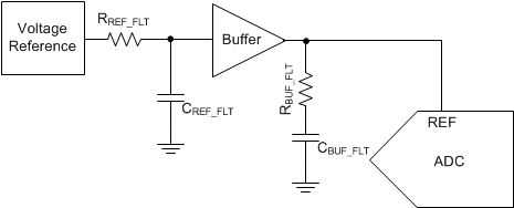
The device operates with an external reference voltage and switches binary-weighted capacitors onto the reference terminal (REF pin) during the conversion process. The switching frequency is proportional to the internal conversion clock frequency but the dynamic charge requirements are a function of the absolute value of the input voltage and reference voltage. This dynamic load must be supported by a reference driver circuit without degrading the noise and linearity performance of the device. During the acquisition process, the device automatically powers down and does not take any dynamic current from the external reference source. The basic circuit diagram for such a reference driver circuit for precision ADCs is shown in Figure 46; see the ADC Reference Driver section for more details on the application circuits.
ADS8864 ai_ref_driver_sch_bas557.gifFigure 46. Reference Driver Schematic