SBAS728A November   2016  – June 2017 ADS8900B , ADS8902B , ADS8904B

PRODUCTION DATA.  

  1. Features
  2. Applications
  3. Description
  4. Revision History
  5. Pin Configuration and Functions
  6. Specifications
    1. 6.1 Absolute Maximum Ratings
    2. 6.2 ESD Ratings
    3. 6.3 Recommended Operating Conditions
    4. 6.4 Thermal Information
    5. 6.5 Electrical Characteristics
    6. 6.6 Timing Requirements
    7. 6.7 Switching Characteristics
    8. 6.8 Typical Characteristics
  7. Detailed Description
    1. 7.1 Overview
    2. 7.2 Functional Block Diagram
    3. 7.3 Feature Description
      1. 7.3.1 LDO Module
      2. 7.3.2 Reference Buffer Module
      3. 7.3.3 Converter Module
        1. 7.3.3.1 Sample-and-Hold Circuit
        2. 7.3.3.2 Internal Oscillator
        3. 7.3.3.3 ADC Transfer Function
      4. 7.3.4 Interface Module
    4. 7.4 Device Functional Modes
      1. 7.4.1 RST State
      2. 7.4.2 ACQ State
      3. 7.4.3 CNV State
    5. 7.5 Programming
      1. 7.5.1 Output Data Word
      2. 7.5.2 Data Transfer Frame
      3. 7.5.3 Interleaving Conversion Cycles and Data Transfer Frames
      4. 7.5.4 Data Transfer Protocols
        1. 7.5.4.1 Protocols for Configuring the Device
        2. 7.5.4.2 Protocols for Reading From the Device
          1. 7.5.4.2.1 Legacy, SPI-Compatible (SYS-xy-S) Protocols
          2. 7.5.4.2.2 SPI-Compatible Protocols with Bus Width Options
          3. 7.5.4.2.3 Source-Synchronous (SRC) Protocols
            1. 7.5.4.2.3.1 Output Clock Source Options with SRC Protocols
            2. 7.5.4.2.3.2 Bus Width Options With SRC Protocols
            3. 7.5.4.2.3.3 Output Data Rate Options With SRC Protocols
      5. 7.5.5 Device Setup
        1. 7.5.5.1 Single Device: All multiSPI Options
        2. 7.5.5.2 Single Device: Minimum Pins for a Standard SPI Interface
        3. 7.5.5.3 Multiple Devices: Daisy-Chain Topology
        4. 7.5.5.4 Multiple Devices: Star Topology
    6. 7.6 Register Maps
      1. 7.6.1 Device Configuration and Register Maps
        1. 7.6.1.1 PD_CNTL Register (address = 04h) [reset = 00h]
        2. 7.6.1.2 SDI_CNTL Register (address = 008h) [reset = 00h]
        3. 7.6.1.3 SDO_CNTL Register (address = 0Ch) [reset = 00h]
        4. 7.6.1.4 DATA_CNTL Register (address = 010h) [reset = 00h]
        5. 7.6.1.5 PATN_LSB Register (address = 014h) [reset = 00h]
        6. 7.6.1.6 PATN_MID Register (address = 015h) [reset = 00h]
        7. 7.6.1.7 PATN_MSB Register (address = 016h) [reset = 00h]
        8. 7.6.1.8 OFST_CAL Register (address = 020h) [reset = 00h]
        9. 7.6.1.9 REF_MRG Register (address = 030h) [reset = 00h]
  8. Application and Implementation
    1. 8.1 Application Information
      1. 8.1.1 ADC Reference Driver
      2. 8.1.2 ADC Input Driver
        1. 8.1.2.1 Charge-Kickback Filter
        2. 8.1.2.2 Input Amplifier Selection
    2. 8.2 Typical Application
      1. 8.2.1 Data Acquisition (DAQ) Circuit for Lowest Distortion and Noise Performance With Differential Input
        1. 8.2.1.1 Design Requirements
        2. 8.2.1.2 Detailed Design Procedure
        3. 8.2.1.3 Application Curves
      2. 8.2.2 DAQ Circuit With FDA Input Driver and Single-Ended or Differential Input
      3. 8.2.3 Design Requirements
      4. 8.2.4 Detailed Design Procedure
      5. 8.2.5 Application Curves
  9. Power-Supply Recommendations
  10. 10Layout
    1. 10.1 Layout Guidelines
      1. 10.1.1 Signal Path
      2. 10.1.2 Grounding and PCB Stack-Up
      3. 10.1.3 Decoupling of Power Supplies
      4. 10.1.4 Reference Decoupling
      5. 10.1.5 Differential Input Decoupling
    2. 10.2 Layout Example
  11. 11Device and Documentation Support
    1. 11.1 Documentation Support
      1. 11.1.1 Related Documentation
    2. 11.2 Related Links
    3. 11.3 Receiving Notification of Documentation Updates
    4. 11.4 Community Resources
    5. 11.5 Trademarks
    6. 11.6 Electrostatic Discharge Caution
    7. 11.7 Glossary
  12. 12Mechanical, Packaging, and Orderable Information

Package Options

Mechanical Data (Package|Pins)
Thermal pad, mechanical data (Package|Pins)
Orderable Information

Power-Supply Recommendations

The devices have two separate power supplies: RVDD and DVDD. The internal reference buffer and the internal LDO operate on RVDD. The ADC core operates on the LDO output (available on the DECAP pins). DVDD is used for the interface circuits. RVDD and DVDD can be independently set to any value within their permissible ranges.

The RVDD supply voltage value defines the permissible range for the external reference voltage VREF on REFIN pin as:

Equation 19. 2.5 V ≤ VREF ≤ (RVDD – 0.3) V

In other words, to use the external reference voltage of VREF, set RVDD so that:

Equation 20. 3 V ≤ RVDD ≤ (VREF + 0.3) V

Place a 10-µF decoupling capacitor between the RVDD and GND pins, and between the DVDD and GND pins, as shown in Figure 120. Use a minimum 1-µF decoupling capacitor between the DECAP pins and the GND pin.
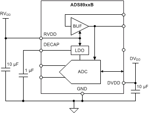
ADS8900B ADS8902B ADS8904B power_sbas707.gif Figure 120. Power-Supply Decoupling