7 Specifications
7.1 Absolute Maximum Ratings(1)
at 25°C free-air temperature (unless otherwise noted)
|
|
MIN |
MAX |
UNIT |
| VCC |
Supply Voltage |
|
-0.3 |
18 |
V |
| VCC_(OX) |
Output supply voltage(2) |
|
-0.3 |
18 |
V |
| VOUT(X) |
Opamp voltage(2) |
|
-0.3 |
18 |
V |
| VIN(X) |
Positive and negative input to GND voltage (2) |
|
-0.3 |
18 |
V |
| IOTF |
Over Temperature Flag pin maximum Current |
|
|
20 |
mA |
| VOTF |
Over Temperature Flag pin maximum Voltage |
|
0 |
7 |
V |
| ISC |
Continuous output short current per opamp |
|
|
Internally Limited |
mA |
| Figure 6 |
| TA |
Operating free-air temperature range |
|
–40 |
125 |
°C |
| TJ |
Operating virtual junction temperature(3) |
|
-40 |
150 |
°C |
| Tstg |
Storage temperature range |
|
–65 |
150 |
°C |
(1) Stresses beyond those listed under "absolute maximum ratings" may cause permanent damage to the device. These are stress ratings only, and functional operation of the device at these or any other conditions beyond those indicated under "recommended operating conditions" is not implied. Exposure to absolute-maximum-rated conditions for extended periods may affect device reliability.
(2) All voltage values are with respect to the GND/substrate terminal, unless otherwise noted.
(3) Maximum power dissipation is a function of TJ(max), θJA, and TA. The maximum allowable power dissipation at any allowable ambient temperature is PD = (TJ(max) – TA)/θJA. Operating at the absolute maximum TJ of 150°C can affect reliability.
7.2 Thermal Information
| THERMAL METRIC(1) |
ALM2402Q1 |
UNIT |
| DRR (SON) |
PWP (HTSSOP) |
| 12 Pins |
14 Pins |
| θJA |
Junction-to-ambient thermal resistance |
39.2 |
46.5 |
°C/W |
| θJCtop |
Junction-to-case (top) thermal resistance |
34.5 |
33.0 |
°C/W |
| θJB |
Junction-to-board thermal resistance |
15.0 |
27.6 |
°C/W |
| ψJT |
Junction-to-top characterization parameter |
0.3 |
1.5 |
°C/W |
| ψJB |
Junction-to-board characterization parameter |
15.2 |
27.4 |
°C/W |
| θJCbot |
Junction-to-case (bottom) thermal resistance |
4.2 |
2.2 |
°C/W |
(1) For more information about traditional and new thermal metrics, see the IC Package Thermal Metrics application report,
SPRA953.
7.3 ESD Ratings
|
VALUE |
UNIT |
| V(ESD) |
Electrostatic discharge |
Human-body model (HBM), per ANSI/ESDA/JEDEC JS-001(1) |
±2000 |
V |
| Charged-device model (CDM), per JEDEC specification JESD22-C101(2) |
DRR |
±750 |
| PWP |
±250 |
(1) JEDEC document JEP155 states that 500-V HBM allows safe manufacturing with a standard ESD control process. Manufacturing with less than 500-V HBM is possible with the necessary precautions.
(2) JEDEC document JEP157 states that 250-V CDM allows safe manufacturing with a standard ESD control process. Manufacturing with less than 250-V CDM is possible with the necessary precautions.
7.4 Recommended Operating Conditions
TA= 25°C
|
MIN |
MAX |
UNIT |
| TJ |
Junction Temperature |
-40 |
150 |
°C |
| TA |
Ambient Temperature |
-40 |
125 |
| IOUT(1) |
Continuous output current (sourcing) |
|
400 |
mA |
| Continuous output current (sinking) |
|
400 |
| VIH_OTF |
OTF input high voltage (Opamp "On" or full operation state) |
1.0 |
|
V |
| VIL_OTF |
OTF input low voltage (Opamp "Off" or shutdown state) |
|
0.35 |
| VIN(X) |
Positive and negative input to GND voltage |
0 |
7 |
| VOTF |
Over Temperature Flag pin maximum Voltage |
2 |
5 |
| VCC |
Input Vcc |
4.5 |
16 |
| VCC_O(X) |
Output Vcc |
3 |
16 |
(1) Current Limit must taken into consideration when choosing maximum output current
7.5 Electrical Characteristics
VOTF = 5 V, VCC = VCC_O1 = VCC_O2 = 5 V and 12 V; TA = –40°C to 125°C; Typical Values at TA = 25°C, unless otherwise noted
| PARAMETER |
TEST CONDITIONS |
MIN |
TYP |
MAX |
UNIT |
| VIO |
Input Offset Voltage (2) |
VICM = Vcc/2, RL = 10 kΩ |
|
1 |
15 |
mV |
| IIB |
Input Bias Current (2) |
VICM = Vcc/2 |
|
1.5 |
100 |
nA |
| IIOS |
Input Offset Current (2) |
VICM = Vcc/2 |
|
|
30 |
nA |
| VICM |
Input Common Mode Range (2) |
VCC = 5.0 |
0.2 |
|
Vcc-1.2 |
V |
| VCC = 12.0 V |
0.2 |
|
7 |
| ICC |
Total Supply Current (both amplifiers)(2) |
IO = 0 A |
|
5 |
15 |
mA |
| VOTF = 0V |
|
0.5(4) |
|
| Vo |
Positive Output Swing |
VCC = VCC_O(X) = 5.0 V; VICM = Vcc/2; VID = 100 mV |
ISINK = 200 mA |
4.7 |
4.87 |
|
V |
| ISINK = 100 mA |
4.85 |
4.94 |
|
| Negative Output Swing |
VCC = VCC_O(X) = 5.0 V; VICM = Vcc/2; VID = 100 mV |
ISOURCE = 200 mA |
|
200 |
425 |
mV |
| ISOURCE = 100 mA |
|
100 |
200 |
| OTF |
Over Temp. Fault and Shutdown(1) |
|
157 |
165 |
175 |
°C |
| VOL_OTF |
Over Temp. Fault low voltage |
Rpullup = 2.5 kΩ, Vpullup = 5.0 V |
|
|
450 |
mV |
| ILIMIT |
Short to Supply Limit (low-side limit)(3) |
|
|
550 |
|
mA |
| Short to Ground Limit (high-side limit)(2)(3) |
|
|
750 |
|
| PSRR |
Power Supply Rejection Ratio(2) |
VCC = 5.0 V to 12 V, RL = 10 kΩ, VICM = Vcc/2, VO = Vcc/2 |
65 |
90 |
|
dB |
| CMRR |
Common Mode Rejection Ratio(2) |
VICM = VICM(min) to VICM(max), RL = 10 kΩ, VO = Vcc/2 |
45 |
90 |
|
dB |
| AVD |
DC Voltage Gain(2) |
RL = 10 kΩ, VICM = Vcc/2, VO = 0.3 V to Vcc-1.5 |
70 |
90 |
|
dB |
(2) Tested and verified in closed loop negative feedback configuration.
(3) This is the static current limit. It can be temporarily higher in applications due to internal propagation delay.
(4) Verified by design.
7.6 AC Characteristics
TJ= –40°C to 125°C; Typical Values at TA = TJ = 25°C; VCC = VCC_O1 = VCC_O2 = 5.0 V and 12 V; VICM=VCC/2
| PARAMETER |
TEST CONDITIONS |
MIN |
TYP |
MAX |
UNIT |
| GBW |
Gain Bandwidth |
CL=15 pF RL=10 kΩ |
|
600 |
|
KHz |
| PM |
Phase Margin |
CL=200 nF RL= 50 Ω |
|
50 |
|
° |
| GM |
Gain Margin |
CL=200 nF RL= 50 Ω |
|
17 |
|
dB |
| SR |
Slew Rate |
G = +1; CL=50 pF; 3 V step |
|
0.17 |
|
V/us |
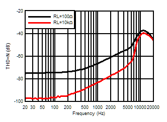
| THD + N |
Total Harmonic Distortion + Noise |
AV = 2 V/V, RL = 100 Ω, Vo = 8 Vpp, Vcc = 12 V, F = 1 kHz, VICM = Vcc/2 |
|
-80 |
|
dB |
| en |
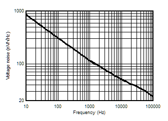
Input Voltage Noise Density |
Vcc = 5 V, F = 1kHz, VICM = Vcc/2 |
|
110 |
|
nV/√HZ |
7.7 Typical Characteristics
TA= 25°C and VCC = VCC_O(X)
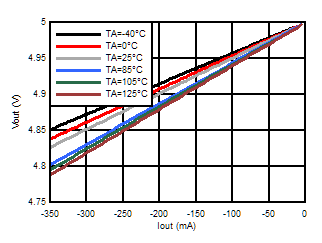
 Figure 1. VOH at VCC = 5 V
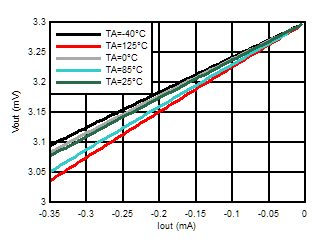
 Figure 3. VOH at VCC = 3.3 V
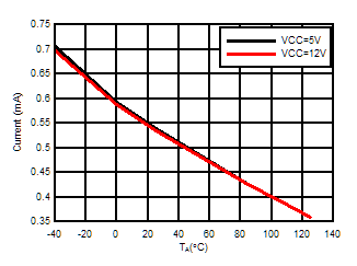
 Figure 5. Short to Supply Current Limit vs. Temperature
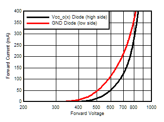
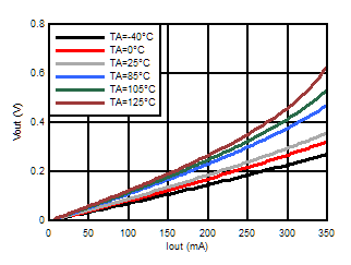
 Figure 7. PMOS (High Side) and NMOS (Low Side) Output Diode Forward Voltage
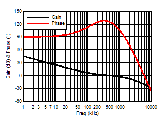
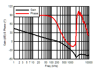
 Figure 9. Gain and Phase (CL = 50 pF and RL = 10 kΩ)
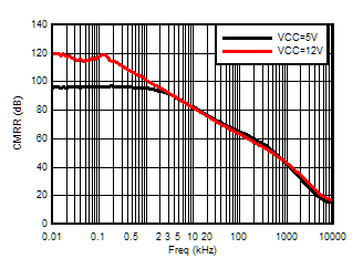
 Figure 11. CMRR vs. Frequency
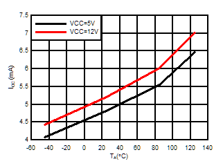
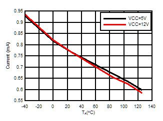
 Figure 13. ICC vs. Temperature
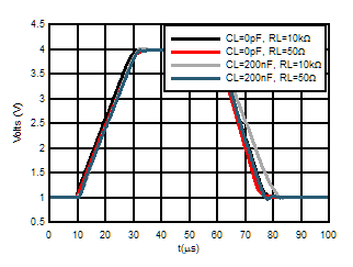
 Figure 15. Slew Rate
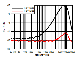
 Figure 17. THD + Noise (Vcc = 12 V)
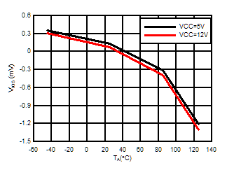
 Figure 19. Input Offset vs. Temperature
 Figure 21. . Input Voltage Noise Spectral Density vs. Frequency
 Figure 2. VOL at VCC = 5 V
 Figure 4. VOL at VCC = 3.3 V
 Figure 6. Short to Groung Current Limit vs. Temperature
 Figure 8. Gain and Phase (CL = 200 nF and RL = 50 Ω)
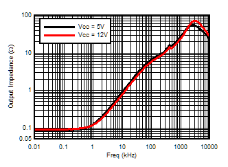
 Figure 10. Output Impedance vs. Frequency
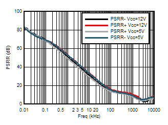
 Figure 12. PSRR vs. Frequency
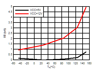
 Figure 14. Input Bias Current vs. Temperature
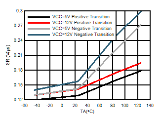
 Figure 16. Slew Rate vs. Temperature
 Figure 18. THD + Noise (Vcc = 5 V)

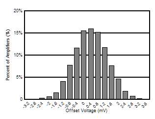
| Vcc =12 V and 5 V |
Vcm = Vcc/2 |
|
Figure 20. Offset Voltage Production Distribution
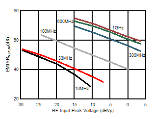
 Figure 22. EMIRR vs. Power
