SPRS710E November 2010 – March 2014 AM1802
PRODUCTION DATA.
- 1AM1802 ARM Microprocessor
- 2Revision History
-
3Device Overview
- 3.1 Device Characteristics
- 3.2 Device Compatibility
- 3.3 ARM Subsystem
- 3.4 Memory Map Summary
- 3.5 Pin Assignments
- 3.6 Pin Multiplexing Control
- 3.7
Terminal Functions
- 3.7.1 Device Reset and JTAG
- 3.7.2 High-Frequency Oscillator and PLL
- 3.7.3 Real-Time Clock and 32-kHz Oscillator
- 3.7.4 DEEPSLEEP Power Control
- 3.7.5 External Memory Interface A (EMIFA)
- 3.7.6 DDR2/mDDR Memory Controller
- 3.7.7 Serial Peripheral Interface Modules (SPI)
- 3.7.8 Boot
- 3.7.9 Universal Asynchronous Receiver/Transmitters (UART0, UART1, UART2)
- 3.7.10 Inter-Integrated Circuit Modules (I2C0)
- 3.7.11 Timers
- 3.7.12 Multichannel Audio Serial Ports (McASP)
- 3.7.13 Universal Serial Bus Modules (USB0)
- 3.7.14 Ethernet Media Access Controller (EMAC)
- 3.7.15 Multimedia Card/Secure Digital (MMC/SD)
- 3.7.16 General Purpose Input Output
- 3.7.17 Reserved and No Connect
- 3.7.18 Supply and Ground
- 3.8 Unused Pin Configurations
- 4Device Configuration
-
5Specifications
- 5.1 Absolute Maximum Ratings Over Operating Junction Temperature Range (Unless Otherwise Noted)
- 5.2 Handling Ratings
- 5.3 Recommended Operating Conditions
- 5.4 Notes on Recommended Power-On Hours (POH)
- 5.5 Electrical Characteristics Over Recommended Ranges of Supply Voltage and Operating Junction Temperature (Unless Otherwise Noted)
-
6Peripheral Information and Electrical Specifications
- 6.1 Parameter Information
- 6.2 Recommended Clock and Control Signal Transition Behavior
- 6.3 Power Supplies
- 6.4 Reset
- 6.5 Crystal Oscillator or External Clock Input
- 6.6 Clock PLLs
- 6.7 Interrupts
- 6.8 Power and Sleep Controller (PSC)
- 6.9 EDMA
- 6.10 External Memory Interface A (EMIFA)
- 6.11
DDR2/mDDR Controller
- 6.11.1 DDR2/mDDR Memory Controller Electrical Data/Timing
- 6.11.2 DDR2/mDDR Controller Register Description(s)
- 6.11.3
DDR2/mDDR Interface
- 6.11.3.1 DDR2/mDDR Interface Schematic
- 6.11.3.2 Compatible JEDEC DDR2/mDDR Devices
- 6.11.3.3 PCB Stackup
- 6.11.3.4 Placement
- 6.11.3.5 DDR2/mDDR Keep Out Region
- 6.11.3.6 Bulk Bypass Capacitors
- 6.11.3.7 High-Speed Bypass Capacitors
- 6.11.3.8 Net Classes
- 6.11.3.9 DDR2/mDDR Signal Termination
- 6.11.3.10 VREF Routing
- 6.11.3.11 DDR2/mDDR CK and ADDR_CTRL Routing
- 6.11.3.12 MDDR/DDR2 Boundary Scan Limitations
- 6.12 Memory Protection Units
- 6.13 MMC / SD / SDIO (MMCSD0)
- 6.14 Multichannel Audio Serial Port (McASP)
- 6.15 Serial Peripheral Interface Ports (SPI0, SPI1)
- 6.16 Inter-Integrated Circuit Serial Ports (I2C)
- 6.17 Universal Asynchronous Receiver/Transmitter (UART)
- 6.18 Universal Serial Bus OTG Controller (USB0) [USB2.0 OTG]
- 6.19 Ethernet Media Access Controller (EMAC)
- 6.20 Management Data Input/Output (MDIO)
- 6.21 Timers
- 6.22 Real Time Clock (RTC)
- 6.23 General-Purpose Input/Output (GPIO)
- 6.24 Emulation Logic
- 7Device and Documentation Support
- 8Mechanical Packaging and Orderable Information
Package Options
Refer to the PDF data sheet for device specific package drawings
Mechanical Data (Package|Pins)
- ZCE|361
- ZWT|361
Thermal pad, mechanical data (Package|Pins)
Orderable Information
6 Peripheral Information and Electrical Specifications
6.1 Parameter Information
6.1.1 Parameter Information Device-Specific Information
Input requirements in this data sheet are tested with an input slew rate of < 4 Volts per nanosecond (4 V/ns) at the device pin and the input signals are driven between 0V and the appropriate IO supply rail for the signal.
The load capacitance value stated is only for characterization and measurement of AC timing signals. This load capacitance value does not indicate the maximum load the device is capable of driving.
6.1.1.1 Signal Transition Levels
All input and output timing parameters are referenced to Vref for both "0" and "1" logic levels.
For 3.3 V I/O, Vref = 1.65 V.
For 1.8 V I/O, Vref = 0.9 V.
For 1.2 V I/O, Vref = 0.6 V.
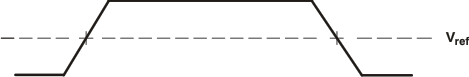 Figure 6-2 Input and Output Voltage Reference Levels for AC Timing Measurements
All rise and fall transition timing parameters are referenced to VIL MAX and VIH MIN for input clocks, VOLMAX and VOH MIN for output clocks.
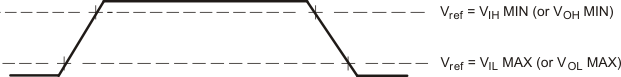 Figure 6-3 Rise and Fall Transition Time Voltage Reference Levels
6.2 Recommended Clock and Control Signal Transition Behavior
All clocks and control signals must transition between VIH and VIL (or between VIL and VIH) in a monotonic manner.
6.3 Power Supplies
6.3.1 Power-On Sequence
The device should be powered-on in the following order:
- RTC (RTC_CVDD) may be powered from an external device (such as a battery) prior to all other supplies being applied or powered-up at the same time as CVDD. If the RTC is not used, RTC_CVDD should be connected to CVDD. RTC_CVDD should not be left unpowered while CVDD is powered.
- Core logic supplies:
- All variable 1.2V - 1.0V core logic supplies (CVDD)
- All static core logic supplies (RVDD, PLL0_VDDA, PLL1_VDDA, USB_CVDD). If voltage scaling is not used on the device, groups 2a) and 2b) can be controlled from the same power supply and powered up together.
- All static 1.8V IO supplies (DVDD18, DDR_DVDD18, USB0_VDDA18) and any of the LVCMOS IO supply groups used at 1.8V nominal (DVDD3318_A, DVDD3318_B, or DVDD3318_C).
- All analog 3.3V PHY supplies (USB0_VDDA33; this is not required if USB0 is not used) and any of the LVCMOS IO supply groups used at 3.3V nominal (DVDD3318_A, DVDD3318_B, or DVDD3318_C).
There is no specific required voltage ramp rate for any of the supplies as long as the LVCMOS supplies operated at 3.3V (DVDD3318_A, DVDD3318_B, or DVDD3318_C) never exceed the STATIC 1.8V supplies by more than 2 volts.
RESET must be maintained active until all power supplies have reached their nominal values.
6.3.2 Power-Off Sequence
The power supplies can be powered-off in any order as long as LVCMOS supplies operated at 3.3V (DVDD3318_A, DVDD3318_B, or DVDD3318_C) never exceed static 1.8V supplies by more than 2 volts. There is no specific required voltage ramp down rate for any of the supplies (except as required to meet the above mentioned voltage condition).
6.4 Reset
6.4.1 Power-On Reset (POR)
A power-on reset (POR) is required to place the device in a known good state after power-up. Power-On Reset is initiated by bringing RESET and TRST low at the same time. POR sets all of the device internal logic to its default state. All pins are tri-stated with the exception of RESETOUT which remains active through the reset sequence, and RTCK/GP8[0]. If an emulator is driving TCK into the device during reset, then RTCK/GP8[0] will drive out RTCK. If TCK is not being driven into the device during reset, then RTCK/GP8[0] will drive low. RESETOUT in an output for use by other controllers in the system that indicates the device is currently in reset.
While both TRST and RESET need to be asserted upon power up, only RESET needs to be released for the device to boot properly. TRST may be asserted indefinitely for normal operation, keeping the JTAG port interface and device's emulation logic in the reset state.
TRST only needs to be released when it is necessary to use a JTAG controller to debug the device or exercise the device's boundary scan functionality. Note: TRST is synchronous and must be clocked by TCK; otherwise, the boundary scan logic may not respond as expected after TRST is asserted.
RESET must be released only in order for boundary-scan JTAG to read the variant field of IDCODE correctly. Other boundary-scan instructions work correctly independent of current state of RESET. For maximum reliability, the device includes an internal pulldown on the TRST pin to ensure that TRST will always be asserted upon power up and the device's internal emulation logic will always be properly initialized.
JTAG controllers from Texas Instruments actively drive TRST high. However, some third-party JTAG controllers may not drive TRST high but expect the use of a pullup resistor on TRST. When using this type of JTAG controller, assert TRST to intialize the device after powerup and externally drive TRST high before attempting any emulation or boundary scan operations.
RTCK/GP8[0] is maintained active through a POR.
A summary of the effects of Power-On Reset is given below:
- All internal logic (including emulation logic and the PLL logic) is reset to its default state
- Internal memory is not maintained through a POR
- RESETOUT goes active
- All device pins go to a high-impedance state
- The RTC peripheral is not reset during a POR. A software sequence is required to reset the RTC
CAUTION: A watchdog reset triggers a POR.
6.4.2 Warm Reset
A warm reset provides a limited reset to the device. Warm Reset is initiated by bringing only RESET low (TRST is maintained high through a warm reset). Warm reset sets certain portions of the device to their default state while leaving others unaltered. All pins are tri-stated with the exception of RESETOUT which remains active through the reset sequence, and RTCK/GP8[0]. If an emulator is driving TCK into the device during reset, then RTCK/GP8[0] will drive out RTCK. If TCK is not being driven into the device during reset, then RTCK/GP8[0] will drive low. RESETOUT is an output for use by other controllers in the system that indicates the device is currently in reset.
During an emulation, the emulator will maintain TRST high and hence only warm reset (not POR) is available during emulation debug and development.
RTCK/GP8[0] is maintained active through a warm reset.
A summary of the effects of Warm Reset is given below:
- All internal logic (except for the emulation logic and the PLL logic) is reset to its default state
- Internal memory is maintained through a warm reset
- RESETOUT goes active
- All device pins go to a high-impedance state
- The RTC peripheral is not reset during a warm reset. A software sequence is required to reset the RTC
6.4.3 Reset Electrical Data Timings
Table 6-1 assumes testing over the recommended operating conditions.
Table 6-1 Reset Timing Requirements ((1), (2))
| NO. | 1.2V | 1.1V | 1.0V | UNIT | |||||
|---|---|---|---|---|---|---|---|---|---|
| MIN | MAX | MIN | MAX | MIN | MAX | ||||
| 1 | tw(RSTL) | Pulse width, RESET/TRST low | 100 | 100 | 100 | ns | |||
| 2 | tsu(BPV-RSTH) | Setup time, boot pins valid before RESET/TRST high | 20 | 20 | 20 | ns | |||
| 3 | th(RSTH-BPV) | Hold time, boot pins valid after RESET/TRST high | 20 | 20 | 20 | ns | |||
| 4 | td(RSTH-RESETOUTH) | RESET high to RESETOUT high; Warm reset | 4096 | 4096 | 4096 | cycles(3) | |||
| RESET high to RESETOUT high; Power-on Reset | 6169 | 6169 | 6169 | ||||||
| 5 | td(RSTL-RESETOUTL) | Delay time, RESET/TRST low to RESETOUT low | 14 | 16 | 20 | ns | |||
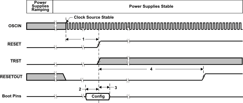 Figure 6-4 Power-On Reset (RESET and TRST active) Timing
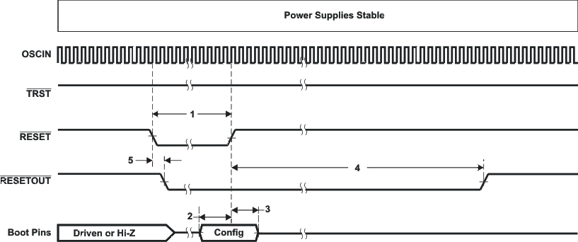 Figure 6-5 Warm Reset (RESET active, TRST high) Timing
6.5 Crystal Oscillator or External Clock Input
The device includes two choices to provide an external clock input, which is fed to the on-chip PLLs to generate high-frequency system clocks. These options are illustrated in Figure 6-6 and Figure 6-7. For input clock frequencies between 12 and 20 MHz, a crystal with 80 ohm max ESR is recommended. For input clock frequencies between 20 and 30 MHz, a crystal with 60 ohm max ESR is recommended. Typical load capacitance values are 10-20 pF, where the load capacitance is the series combination of C1 and C2.
The CLKMODE bit in the PLLCTL register must be 0 to use the on-chip oscillator. If CLKMODE is set to 1, the internal oscillator is disabled.
Figure 6-6 illustrates the option that uses on-chip 1.2V oscillator with external crystal circuit. Figure 6-7 illustrates the option that uses an external 1.2V clock input.
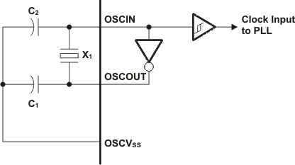 Figure 6-6 On-Chip Oscillator
Table 6-2 Oscillator Timing Requirements
| MIN | MAX | UNIT | ||
|---|---|---|---|---|
| fosc | Oscillator frequency range (OSCIN/OSCOUT) | 12 | 30 | MHz |
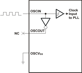 Figure 6-7 External 1.2V Clock Source
Table 6-3 OSCIN Timing Requirements for an Externally Driven Clock
| MIN | MAX | UNIT | ||
|---|---|---|---|---|
| fOSCIN | OSCIN frequency range | 12 | 50 | MHz |
| tc(OSCIN) | Cycle time, external clock driven on OSCIN | 20 | ns | |
| tw(OSCINH) | Pulse width high, external clock on OSCIN | 0.4 tc(OSCIN) | ns | |
| tw(OSCINL) | Pulse width low, external clock on OSCIN | 0.4 tc(OSCIN) | ns | |
| tt(OSCIN) | Transition time, OSCIN | 0.25P or 10 (1) | ns | |
| tj(OSCIN) | Period jitter, OSCIN | 0.02P | ns | |
6.6 Clock PLLs
The device has two PLL controllers that provide clocks to different parts of the system. PLL0 provides clocks (though various dividers) to most of the components of the device. PLL1 provides clocks to the mDDR/DDR2 Controller and provides an alternate clock source for the ASYNC3 clock domain. This allows the peripherals on the ASYNC3 clock domain to be immune to frequency scaling operation on PLL0.
The PLL controller provides the following:
- Glitch-Free Transitions (on changing clock settings)
- Domain Clocks Alignment
- Clock Gating
- PLL power down
The various clock outputs given by the controller are as follows:
- Domain Clocks: SYSCLK [1:n]
- Auxiliary Clock from reference clock source: AUXCLK
Various dividers that can be used are as follows:
- Post-PLL Divider: POSTDIV
- SYSCLK Divider: D1, ¼, Dn
Various other controls supported are as follows:
- PLL Multiplier Control: PLLM
- Software programmable PLL Bypass: PLLEN
6.6.1 PLL Device-Specific Information
The PLL requires some external filtering components to reduce power supply noise as shown in Figure 6-8.
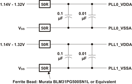 Figure 6-8 PLL External Filtering Components
The external filtering components shown above provide noise immunity for the PLLs. PLL0_VDDA and PLL1_VDDA should not be connected together to provide noise immunity between the two PLLs. Likewise, PLL0_VSSA and PLL1_VSSA should not be connected together.
The input to the PLL is either from the on-chip oscillator or from an external clock on the OSCIN pin. PLL0 outputs seven clocks that have programmable divider options. PLL1 outputs three clocks that have programmable divider options. Figure 6-9 illustrates the high-level view of the PLL Topology.
The PLLs are disabled by default after a device reset. They must be configured by software according to the allowable operating conditions listed in Table 6-4 before enabling the device to run from the PLL by setting PLLEN = 1.
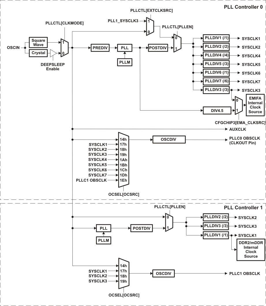 Figure 6-9 PLL Topology
Table 6-4 Allowed PLL Operating Conditions (PLL0 and PLL1)
| NO. | PARAMETER | Default Value |
MIN | MAX | UNIT |
|---|---|---|---|---|---|
| 1 | PLLRST: Assertion time during initialization | N/A | 1000 | N/A | ns |
| 2 | Lock time: The time that the application has to wait for the PLL to acquire lock before setting PLLEN, after changing PREDIV, PLLM, or OSCIN | N/A | N/A | 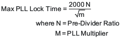 |
OSCIN cycles |
| 3 | PREDIV: Pre-divider value | /1 | /1 | /32 | |
| 4 | PLLREF: PLL input frequency | 12 | 30 (if internal oscillator is used) 50 (if external clock source is used) |
MHz | |
| 5 | PLLM: PLL multiplier values(1) | x20 | x4 | x32 | |
| 6 | PLLOUT: PLL output frequency | N/A | 300 | 600 | MHz |
| 7 | POSTDIV: Post-divider value | /1 | /1 | /32 |
6.6.2 Device Clock Generation
PLL0 is controlled by PLL Controller 0 and PLL1 is controlled by PLL Controller 1. PLLC0 and PLLC1 manage the clock ratios, alignment, and gating for the system clocks to the chip. The PLLCs are responsible for controlling all modes of the PLL through software, in terms of pre-division of the clock inputs (PLLC0 only), multiply factors within the PLLs, and post-division for each of the chip-level clocks from the PLLs outputs. PLLC0 also controls reset propagation through the chip, clock alignment, and test points.
PLLC0 provides clocks for the majority of the system but PLLC1 provides clocks to the mDDR/DDR2 Controller and the ASYNC3 clock domain to provide frequency scaling immunity to a defined set or peripherals. The ASYNC3 clock domain can either derive its clock from PLL1_SYSCLK2 (for frequency scaling immunity from PLL0) or from PLL0_SYSCLK2 (for synchronous timing with PLL0) depending on the application requirements. In addition, some peripherals have specific clock options independent of the ASYNC clock domain.
6.6.3 Dynamic Voltage and Frequency Scaling (DVFS)
The processor supports multiple operating points by scaling voltage and frequency to minimize power consumption for a given level of processor performance.
Frequency scaling is achieved by modifying the setting of the PLL controllers’ multipliers, post-dividers (POSTDIV), and system clock dividers (SYSCLKn). Modification of the POSTDIV and SYSCLK values does not require relocking the PLL and provides lower latency to switch between operating points, but at the expense of the frequencies being limited by the integer divide values (only the divide values are altered the PLL multiplier is left unmodified). Non integer divide frequency values can be achieved by changing both the multiplier and the divide values, but when the PLL multiplier is changed the PLL must relock, incurring additional latency to change between operating points. Detailed information on modifying the PLL Controller settings can be found in the AM1802 ARM Microprocessor System Reference Guide (literature number SPRUGX5).
Voltage scaling is enabled from outside the device by controlling an external voltage regulator. The processor may communicate with the regulator using GPIOs, I2C or some other interface. When switching between voltage-frequency operating points, the voltage must always support the desired frequency. When moving from a high-performance operating point to a lower performance operating point, the frequency should be lowered first followed by the voltage. When moving from a low-performance operating point to a higher performance operating point, the voltage should be raised first followed by the frequency. Voltage operating points refer to the CVdd voltage at that point. Other static supplies must be maintained at their nominal voltages at all operating points.
The maximum voltage slew rate for CVdd supply changes is 1 mV/us.
For additional information on power management solutions from TI for this processor, follow the Power Management link in the Product Folder on www.ti.com for this processor.
The processor supports multiple clock domains some of which have clock ratio requirements to each other. PLL0_SYSCLK2:PLL0_SYSCLK4:PLL0_SYSCLK6 are synchronous to each other and the SYSCLKn dividers must always be configured such that the ratio between these domains is 2:4:1. The ASYNC and ASYNC3 clock domains are asynchronous to the other clock domains and have no specific ratio requirement.
The table below summarizes the maximum internal clock frequencies at each of the voltage operating points.
Table 6-5 Maximum Internal Clock Frequencies at Each Voltage Operating Point
| CLOCK SOURCE | CLOCK DOMAIN | 1.2V NOM | 1.1V NOM | 1.0V NOM | |
|---|---|---|---|---|---|
| PLL0_SYSCLK1 | Not used on this processor | - | - | - | |
| PLL0_SYSCLK2 | SYSCLK2 clock domain peripherals and optional clock source for ASYNC3 clock domain peripherals | 150 MHz | 100 MHz | 50 MHz | |
| PLL0_SYSCLK3 | Optional clock for ASYNC1 clock domain | ||||
| PLL0_SYSCLK4 | SYSCLK4 domain peripherals | 75 MHz | 50 MHz | 25 MHz | |
| PLL0_SYSCLK5 | Not used on this processor | - | - | - | |
| PLL0_SYSCLK6 | ARM subsystem | 300 MHz | 200 MHz | 100 MHz | |
| PLL0_SYSCLK7 | Optional 50 MHz clock source for EMAC RMII interface | 50 MHz | - | - | |
| PLL1_SYSCLK1 | DDR2/mDDR Interface clock source (memory interface clock is one-half of the value shown) | 312 MHz | 300 MHz | 266 MHz | |
| PLL1_SYSCLK2 | Optional clock source for ASYNC3 clock domain peripherals | 150 MHz | 100 MHz | 75 MHz | |
| PLL1_SYSCLK3 | Alternate clock source input to PLL Controller 0 | 75 MHz | 75 MHz | 75 MHz | |
| McASP AUXCLK | Bypass clock source for the McASP | 50 MHz | 50 MHz | 50 MHz | |
| PLL0_AUXCLK | Bypass clock source for the USB0 | 48 MHz | 48 MHz | 48 MHz | |
| ASYNC1 | ASYNC1 Clock Domain (EMIFA) | Async Mode | 148 MHz | 75 MHz | 50 MHz |
| SDRAM Mode | 100 MHz | 66.6 MHz | 50 MHz | ||
| ASYNC2 | ASYNC2 Clock Domain (multiple peripherals) | 50 MHz | 50 MHz | 50 MHz | |
Some interfaces have specific limitations on supported modes/speeds at each operating point. See the corresponding peripheral sections of this document for more information.
TI provides software components (called the Power Manager) to perform DVFS and abstract the task from the user. The Power Manager controls changing operating points (both frequency and voltage) and handles the related tasks involved such as informing/controlling peripherals to provide graceful transitions between operating points.
6.7 Interrupts
6.7.1 ARM CPU Interrupts
The ARM9 CPU core supports 2 direct interrupts: FIQ and IRQ. The ARM Interrupt Controller (AINTC) extends the number of interrupts to 100, and provides features like programmable masking, priority, hardware nesting support, and interrupt vector generation.
6.7.1.1 ARM Interrupt Controller (AINTC) Interrupt Signal Hierarchy
The ARM Interrupt controller organizes interrupts into the following hierarchy:
- Peripheral Interrupt Requests
- Individual Interrupt Sources from Peripherals
- 101 System Interrupts
- One or more Peripheral Interrupt Requests are combined (fixed configuration) to generate a System Interrupt.
- After prioritization, the AINTC will provide an interrupt vector based unique to each System Interrupt
- 32 Interrupt Channels
- Each System Interrupt is mapped to one of the 32 Interrupt Channels
- Channel Number determines the first level of prioritization, Channel 0 is highest priority and 31 lowest.
- If more than one system interrupt is mapped to a channel, priority within the channel is determined by system interrupt number (0 highest priority)
- Host Interrupts (FIQ and IRQ)
- Interrupt Channels 0 and 1 generate the ARM FIQ interrupt
- Interrupt Channels 2 through 31 Generate the ARM IRQ interrupt
- Debug Interrupts
- Two Debug Interrupts are supported and can be used to trigger events in the debug subsystem
- Sources can be selected from any of the System Interrupts or Host Interrupts
6.7.1.2 AINTC Hardware Vector Generation
The AINTC also generates an interrupt vector in hardware for both IRQ and FIQ host interrupts. This may be used to accelerate interrupt dispatch. A unique vector is generated for each of the 100 system interrupts. The vector is computed in hardware as:
VECTOR = BASE + (SYSTEM INTERRUPT NUMBER × SIZE)
Where BASE and SIZE are programmable. The computed vector is a 32-bit address which may dispatched to using a single instruction of type LDR PC, [PC, #-<offset_12>] at the FIQ and IRQ vector locations (0xFFFF0018 and 0xFFFF001C respectively).
6.7.1.3 AINTC Hardware Interrupt Nesting Support
Interrupt nesting occurs when an interrupt service routine re-enables interrupts, to allow the CPU to interrupt the ISR if a higher priority event occurs. The AINTC provides hardware support to facilitate interrupt nesting. It supports both global and per host interrupt (FIQ and IRQ in this case) automatic nesting. If enabled, the AINTC will automatically update an internal nesting register that temporarily masks interrupts at and below the priority of the current interrupt channel. Then if the ISR re-enables interrupts; only higher priority channels will be able to interrupt it. The nesting level is restored by the ISR by writing to the nesting level register on completion. Support for nesting can be enabled/disabled by software, with the option of automatic nesting on a global or per host interrupt basis; or manual nesting.
6.7.1.4 AINTC System Interrupt Assignments
Table 6-6 AINTC System Interrupt Assignments
| System Interrupt | Interrupt Name | Source |
|---|---|---|
| 0 | COMMTX | ARM |
| 1 | COMMRX | ARM |
| 2 | NINT | ARM |
| 3 | - | Reserved |
| 4 | - | Reserved |
| 5 | - | Reserved |
| 6 | - | Reserved |
| 7 | - | Reserved |
| 8 | - | Reserved |
| 9 | - | Reserved |
| 10 | - | Reserved |
| 11 | EDMA3_0_CC0_INT0 | EDMA3_0 Channel Controller 0 Shadow Region 0 Transfer Completion Interrupt |
| 12 | EDMA3_0_CC0_ERRINT | EDMA3_0 Channel Controller 0 Error Interrupt |
| 13 | EDMA3_0_TC0_ERRINT | EDMA3_0 Transfer Controller 0 Error Interrupt |
| 14 | EMIFA_INT | EMIFA |
| 15 | IIC0_INT | I2C0 |
| 16 | MMCSD0_INT0 | MMCSD0 MMC/SD Interrupt |
| 17 | MMCSD0_INT1 | MMCSD0 SDIO Interrupt |
| 18 | PSC0_ALLINT | PSC0 |
| 19 | RTC_IRQS[1:0] | RTC |
| 20 | SPI0_INT | SPI0 |
| 21 | T64P0_TINT12 | Timer64P0 Interrupt 12 |
| 22 | T64P0_TINT34 | Timer64P0 Interrupt 34 |
| 23 | T64P1_TINT12 | Timer64P1 Interrupt 12 |
| 24 | T64P1_TINT34 | Timer64P1 Interrupt 34 |
| 25 | UART0_INT | UART0 |
| 26 | - | Reserved |
| 27 | MPU_BOOTCFG_ERR | Shared MPU and SYSCFG Address/Protection Error Interrupt |
| 28-31 | - | Reserved |
| 32 | EDMA3_0_TC1_ERRINT | EDMA3_0 Transfer Controller 1 Error Interrupt |
| 33 | EMAC_C0RXTHRESH | EMAC - Core 0 Receive Threshold Interrupt |
| 34 | EMAC_C0RX | EMAC - Core 0 Receive Interrupt |
| 35 | EMAC_C0TX | EMAC - Core 0 Transmit Interrupt |
| 36 | EMAC_C0MISC | EMAC - Core 0 Miscellaneous Interrupt |
| 37 | EMAC_C1RXTHRESH | EMAC - Core 1 Receive Threshold Interrupt |
| 38 | EMAC_C1RX | EMAC - Core 1 Receive Interrupt |
| 39 | EMAC_C1TX | EMAC - Core 1 Transmit Interrupt |
| 40 | EMAC_C1MISC | EMAC - Core 1 Miscellaneous Interrupt |
| 41 | DDR2_MEMERR | DDR2 Controller |
| 42 | GPIO_B0INT | GPIO Bank 0 Interrupt |
| 43 | GPIO_B1INT | GPIO Bank 1 Interrupt |
| 44 | GPIO_B2INT | GPIO Bank 2 Interrupt |
| 45 | GPIO_B3INT | GPIO Bank 3 Interrupt |
| 46 | GPIO_B4INT | GPIO Bank 4 Interrupt |
| 47 | GPIO_B5INT | GPIO Bank 5 Interrupt |
| 48 | GPIO_B6INT | GPIO Bank 6 Interrupt |
| 49 | GPIO_B7INT | GPIO Bank 7 Interrupt |
| 50 | GPIO_B8INT | GPIO Bank 8 Interrupt |
| 51-52 | - | Reserved |
| 53 | UART_INT1 | UART1 |
| 54 | MCASP_INT | McASP0 Combined RX / TX Interrupts |
| 55 | PSC1_ALLINT | PSC1 |
| 56 | SPI1_INT | SPI1 |
| 57 | - | Reserved |
| 58 | USB0_INT | USB0 Interrupt |
| 59-60 | - | Reserved |
| 61 | UART2_INT | UART2 |
| 62-67 | - | Reserved |
| 68 | T64P2_ALL | Timer64P2 - Combined TINT12 and TINT34 |
| 69-73 | - | Reserved |
| 74 | T64P2_CMPINT0 | Timer64P2 - Compare 0 |
| 75 | T64P2_CMPINT1 | Timer64P2 - Compare 1 |
| 76 | T64P2_CMPINT2 | Timer64P2 - Compare 2 |
| 77 | T64P2_CMPINT3 | Timer64P2 - Compare 3 |
| 78 | T64P2_CMPINT4 | Timer64P2 - Compare 4 |
| 79 | T64P2_CMPINT5 | Timer64P2 - Compare 5 |
| 80 | T64P2_CMPINT6 | Timer64P2 - Compare 6 |
| 81 | T64P2_CMPINT7 | Timer64P2 - Compare 7 |
| 82 | T64P3_CMPINT0 | Timer64P3 - Compare 0 |
| 83 | T64P3_CMPINT1 | Timer64P3 - Compare 1 |
| 84 | T64P3_CMPINT2 | Timer64P3 - Compare 2 |
| 85 | T64P3_CMPINT3 | Timer64P3 - Compare 3 |
| 86 | T64P3_CMPINT4 | Timer64P3 - Compare 4 |
| 87 | T64P3_CMPINT5 | Timer64P3 - Compare 5 |
| 88 | T64P3_CMPINT6 | Timer64P3 - Compare 6 |
| 89 | T64P3_CMPINT7 | Timer64P3 - Compare 7 |
| 90 | ARMCLKSTOPREQ | PSC0 |
| 91-92 | - | Reserved |
| 93 | EDMA3_1_CC0_INT0 | EDMA3_1 Channel Controller 0 Shadow Region 0 Transfer Completion Interrupt |
| 94 | EDMA3_1_CC0_ERRINT | EDMA3_1Channel Controller 0 Error Interrupt |
| 95 | EDMA3_1_TC0_ERRINT | EDMA3_1 Transfer Controller 0 Error Interrupt |
| 96 | T64P3_ALL | Timer64P 3 - Combined TINT12 and TINT34 |
| 97-100 | - | Reserved |
6.7.1.5 AINTC Memory Map
Table 6-7 AINTC Memory Map
| BYTE ADDRESS | ACRONYM | DESCRIPTION |
|---|---|---|
| 0xFFFE E000 | REV | Revision Register |
| 0xFFFE E004 | CR | Control Register |
| 0xFFFE E008 - 0xFFFE E00F | - | Reserved |
| 0xFFFE E010 | GER | Global Enable Register |
| 0xFFFE E014 - 0xFFFE E01B | - | Reserved |
| 0xFFFE E01C | GNLR | Global Nesting Level Register |
| 0xFFFE E020 | SISR | System Interrupt Status Indexed Set Register |
| 0xFFFE E024 | SICR | System Interrupt Status Indexed Clear Register |
| 0xFFFE E028 | EISR | System Interrupt Enable Indexed Set Register |
| 0xFFFE E02C | EICR | System Interrupt Enable Indexed Clear Register |
| 0xFFFE E030 | - | Reserved |
| 0xFFFE E034 | HIEISR | Host Interrupt Enable Indexed Set Register |
| 0xFFFE E038 | HIDISR | Host Interrupt Enable Indexed Clear Register |
| 0xFFFE E03C - 0xFFFE E04F | - | Reserved |
| 0xFFFE E050 | VBR | Vector Base Register |
| 0xFFFE E054 | VSR | Vector Size Register |
| 0xFFFE E058 | VNR | Vector Null Register |
| 0xFFFE E05C - 0xFFFE E07F | - | Reserved |
| 0xFFFE E080 | GPIR | Global Prioritized Index Register |
| 0xFFFE E084 | GPVR | Global Prioritized Vector Register |
| 0xFFFE E088 - 0xFFFE E1FF | - | Reserved |
| 0xFFFE E200 | SRSR[0] | System Interrupt Status Raw / Set Registers |
| 0xFFFE E204 | SRSR[1] | |
| 0xFFFE E208 | SRSR[2] | |
| 0xFFFE E20C | SRSR[3] | |
| 0xFFFE E210- 0xFFFE E27F | - | Reserved |
| 0xFFFE E280 | SECR[0] | System Interrupt Status Enabled / Clear Registers |
| 0xFFFE E284 | SECR[1] | |
| 0xFFFE E288 | SECR[2] | |
| 0xFFFE E28C | SECR[3] | |
| 0xFFFE E290 - 0xFFFE E2FF | - | Reserved |
| 0xFFFE E300 | ESR[0] | System Interrupt Enable Set Registers |
| 0xFFFE E304 | ESR[1] | |
| 0xFFFE E308 | ESR[2] | |
| 0xFFFE E30C | ESR[3] | |
| 0xFFFE E310 - 0xFFFE E37F | - | Reserved |
| 0xFFFE E380 | ECR[0] | System Interrupt Enable Clear Registers |
| 0xFFFE E384 | ECR[1] | |
| 0xFFFE E388 | ECR[2] | |
| 0xFFFE E38C | ECR[3] | |
| 0xFFFE E390 - 0xFFFE E3FF | - | Reserved |
| 0xFFFE E400 - 0xFFFE E45B | CMR[0] | Channel Map Registers |
| 0xFFFE E404 | CMR[1] | |
| 0xFFFE E408 | CMR[2] | |
| 0xFFFE E40C | CMR[3] | |
| 0xFFFE E410 | CMR[4] | |
| 0xFFFE E414 | CMR[5] | |
| 0xFFFE E418 | CMR[6] | |
| 0xFFFE E41C | CMR[7] | |
| 0xFFFE E420 | CMR[8] | |
| 0xFFFE E424 | CMR[9] | |
| 0xFFFE E428 | CMR[10] | |
| 0xFFFE E42C | CMR[11] | |
| 0xFFFE E430 | CMR[12] | |
| 0xFFFE E434 | CMR[13] | |
| 0xFFFE E438 | CMR[14] | |
| 0xFFFE E43C | CMR[15] | |
| 0xFFFE E440 | CMR[16] | |
| 0xFFFE E444 | CMR[17] | |
| 0xFFFE E448 | CMR[18] | |
| 0xFFFE E44C | CMR[19] | |
| 0xFFFE E450 | CMR[20] | |
| 0xFFFE E454 | CMR[21] | |
| 0xFFFE E458 | CMR[22] | |
| 0xFFFE E45C | CMR[23] | |
| 0xFFFE E460 | CMR[24] | |
| 0xFFFE E464 | CMR[25] | |
| 0xFFFE E468 - 0xFFFE E8FF | - | Reserved |
| 0xFFFE E900 | HIPIR[0] | Host Interrupt Prioritized Index Registers |
| 0xFFFE E904 | HIPIR[1] | |
| 0xFFFE E908 - 0xFFFE EEFF | - | Reserved |
| 0xFFFE EF00 | DSR[0] | Debug Select Registers |
| 0xFFFE EF04 | DSR[1] | |
| 0xFFFE EF08 - 0xFFFE F0FF | - | Reserved |
| 0xFFFE F100 | HINLR[0] | Host Interrupt Nesting Level Registers |
| 0xFFFE F104 | HINLR[1] | |
| 0xFFFE F108 - 0xFFFE F4FF | - | Reserved |
| 0xFFFE F500 | HIER[0] | Host Interrupt Enable Register |
| 0xFFFE F504 - 0xFFFE F5FF | - | Reserved |
| 0xFFFE F600 | HIPVR[0] - | Host Interrupt Prioritized Vector Registers |
| 0xFFFE F604 | HIPVR[1] | |
| 0xFFFE F608 - 0xFFFE FFFF | - | Reserved |
6.8 Power and Sleep Controller (PSC)
The Power and Sleep Controllers (PSC) are responsible for managing transitions of system power on/off, clock on/off, resets (device level and module level). It is used primarily to provide granular power control for on chip modules (peripherals and CPU). A PSC module consists of a Global PSC (GPSC) and a set of Local PSCs (LPSCs). The GPSC contains memory mapped registers, PSC interrupts, a state machine for each peripheral/module it controls. An LPSC is associated with every module that is controlled by the PSC and provides clock and reset control.
The PSC includes the following features:
- Provides a software interface to:
- Control module clock enable/disable
- Control module reset
- Control CPU local reset
- Supports IcePick emulation features: power, clock and reset
PSC0 controls 16 local PSCs.
PSC1 controls 32 local PSCs.
Table 6-8 Power and Sleep Controller (PSC) Registers
| PSC0 BYTE ADDRESS | PSC1 BYTE ADDRESS | ACRONYM | REGISTER DESCRIPTION |
|---|---|---|---|
| 0x01C1 0000 | 0x01E2 7000 | REVID | Peripheral Revision and Class Information Register |
| 0x01C1 0018 | 0x01E2 7018 | INTEVAL | Interrupt Evaluation Register |
| 0x01C1 0040 | 0x01E2 7040 | MERRPR0 | Module Error Pending Register 0 (module 0-15) (PSC0) |
| Module Error Pending Register 0 (module 0-31) (PSC1) | |||
| 0x01C1 0050 | 0x01E2 7050 | MERRCR0 | Module Error Clear Register 0 (module 0-15) (PSC0) |
| Module Error Clear Register 0 (module 0-31) (PSC1) | |||
| 0x01C1 0060 | 0x01E2 7060 | PERRPR | Power Error Pending Register |
| 0x01C1 0068 | 0x01E2 7068 | PERRCR | Power Error Clear Register |
| 0x01C1 0120 | 0x01E2 7120 | PTCMD | Power Domain Transition Command Register |
| 0x01C1 0128 | 0x01E2 7128 | PTSTAT | Power Domain Transition Status Register |
| 0x01C1 0200 | 0x01E2 7200 | PDSTAT0 | Power Domain 0 Status Register |
| 0x01C1 0204 | 0x01E2 7204 | PDSTAT1 | Power Domain 1 Status Register |
| 0x01C1 0300 | 0x01E2 7300 | PDCTL0 | Power Domain 0 Control Register |
| 0x01C1 0304 | 0x01E2 7304 | PDCTL1 | Power Domain 1 Control Register |
| 0x01C1 0400 | 0x01E2 7400 | PDCFG0 | Power Domain 0 Configuration Register |
| 0x01C1 0404 | 0x01E2 7404 | PDCFG1 | Power Domain 1 Configuration Register |
| 0x01C1 0800 | 0x01E2 7800 | MDSTAT0 | Module 0 Status Register |
| 0x01C1 0804 | 0x01E2 7804 | MDSTAT1 | Module 1 Status Register |
| 0x01C1 0808 | 0x01E2 7808 | MDSTAT2 | Module 2 Status Register |
| 0x01C1 080C | 0x01E2 780C | MDSTAT3 | Module 3 Status Register |
| 0x01C1 0810 | 0x01E2 7810 | MDSTAT4 | Module 4 Status Register |
| 0x01C1 0814 | 0x01E2 7814 | MDSTAT5 | Module 5 Status Register |
| 0x01C1 0818 | 0x01E2 7818 | MDSTAT6 | Module 6 Status Register |
| 0x01C1 081C | 0x01E2 781C | MDSTAT7 | Module 7 Status Register |
| 0x01C1 0820 | 0x01E2 7820 | MDSTAT8 | Module 8 Status Register |
| 0x01C1 0824 | 0x01E2 7824 | MDSTAT9 | Module 9 Status Register |
| 0x01C1 0828 | 0x01E2 7828 | MDSTAT10 | Module 10 Status Register |
| 0x01C1 082C | 0x01E2 782C | MDSTAT11 | Module 11 Status Register |
| 0x01C1 0830 | 0x01E2 7830 | MDSTAT12 | Module 12 Status Register |
| 0x01C1 0834 | 0x01E2 7834 | MDSTAT13 | Module 13 Status Register |
| 0x01C1 0838 | 0x01E2 7838 | MDSTAT14 | Module 14 Status Register |
| 0x01C1 083C | 0x01E2 783C | MDSTAT15 | Module 15 Status Register |
| - | 0x01E2 7840 | MDSTAT16 | Module 16 Status Register |
| - | 0x01E2 7844 | MDSTAT17 | Module 17 Status Register |
| - | 0x01E2 7848 | MDSTAT18 | Module 18 Status Register |
| - | 0x01E2 784C | MDSTAT19 | Module 19 Status Register |
| - | 0x01E2 7850 | MDSTAT20 | Module 20 Status Register |
| - | 0x01E2 7854 | MDSTAT21 | Module 21 Status Register |
| - | 0x01E2 7858 | MDSTAT22 | Module 22 Status Register |
| - | 0x01E2 785C | MDSTAT23 | Module 23 Status Register |
| - | 0x01E2 7860 | MDSTAT24 | Module 24 Status Register |
| - | 0x01E2 7864 | MDSTAT25 | Module 25 Status Register |
| - | 0x01E2 7868 | MDSTAT26 | Module 26 Status Register |
| - | 0x01E2 786C | MDSTAT27 | Module 27 Status Register |
| - | 0x01E2 7870 | MDSTAT28 | Module 28 Status Register |
| - | 0x01E2 7874 | MDSTAT29 | Module 29 Status Register |
| - | 0x01E2 7878 | MDSTAT30 | Module 30 Status Register |
| - | 0x01E2 787C | MDSTAT31 | Module 31 Status Register |
| 0x01C1 0A00 | 0x01E2 7A00 | MDCTL0 | Module 0 Control Register |
| 0x01C1 0A04 | 0x01E2 7A04 | MDCTL1 | Module 1 Control Register |
| 0x01C1 0A08 | 0x01E2 7A08 | MDCTL2 | Module 2 Control Register |
| 0x01C1 0A0C | 0x01E2 7A0C | MDCTL3 | Module 3 Control Register |
| 0x01C1 0A10 | 0x01E2 7A10 | MDCTL4 | Module 4 Control Register |
| 0x01C1 0A14 | 0x01E2 7A14 | MDCTL5 | Module 5 Control Register |
| 0x01C1 0A18 | 0x01E2 7A18 | MDCTL6 | Module 6 Control Register |
| 0x01C1 0A1C | 0x01E2 7A1C | MDCTL7 | Module 7 Control Register |
| 0x01C1 0A20 | 0x01E2 7A20 | MDCTL8 | Module 8 Control Register |
| 0x01C1 0A24 | 0x01E2 7A24 | MDCTL9 | Module 9 Control Register |
| 0x01C1 0A28 | 0x01E2 7A28 | MDCTL10 | Module 10 Control Register |
| 0x01C1 0A2C | 0x01E2 7A2C | MDCTL11 | Module 11 Control Register |
| 0x01C1 0A30 | 0x01E2 7A30 | MDCTL12 | Module 12 Control Register |
| 0x01C1 0A34 | 0x01E2 7A34 | MDCTL13 | Module 13 Control Register |
| 0x01C1 0A38 | 0x01E2 7A38 | MDCTL14 | Module 14 Control Register |
| 0x01C1 0A3C | 0x01E2 7A3C | MDCTL15 | Module 15 Control Register |
| - | 0x01E2 7A40 | MDCTL16 | Module 16 Control Register |
| - | 0x01E2 7A44 | MDCTL17 | Module 17 Control Register |
| - | 0x01E2 7A48 | MDCTL18 | Module 18 Control Register |
| - | 0x01E2 7A4C | MDCTL19 | Module 19 Control Register |
| - | 0x01E2 7A50 | MDCTL20 | Module 20 Control Register |
| - | 0x01E2 7A54 | MDCTL21 | Module 21 Control Register |
| - | 0x01E2 7A58 | MDCTL22 | Module 22 Control Register |
| - | 0x01E2 7A5C | MDCTL23 | Module 23 Control Register |
| - | 0x01E2 7A60 | MDCTL24 | Module 24 Control Register |
| - | 0x01E2 7A64 | MDCTL25 | Module 25 Control Register |
| - | 0x01E2 7A68 | MDCTL26 | Module 26 Control Register |
| - | 0x01E2 7A6C | MDCTL27 | Module 27 Control Register |
| - | 0x01E2 7A70 | MDCTL28 | Module 28 Control Register |
| - | 0x01E2 7A74 | MDCTL29 | Module 29 Control Register |
| - | 0x01E2 7A78 | MDCTL30 | Module 30 Control Register |
| - | 0x01E2 7A7C | MDCTL31 | Module 31 Control Register |
6.8.1 Power Domain and Module Topology
The device includes two PSC modules.
Each PSC module controls clock states for several of the on chip modules, controllers and interconnect components. Table 6-9 and Table 6-10 lists the set of peripherals/modules that are controlled by the PSC, the power domain they are associated with, the LPSC assignment and the default (power-on reset) module states. See the device-specific data manual for the peripherals available on a given device. The module states and terminology are defined in Section 6.8.1.1.
Table 6-9 PSC0 Default Module Configuration
| LPSC Number |
Module Name | Power Domain | Default Module State | Auto Sleep/Wake Only |
|---|---|---|---|---|
| 0 | EDMA3 Channel Controller 0 | AlwaysON (PD0) | SwRstDisable | — |
| 1 | EDMA3 Transfer Controller 0 | AlwaysON (PD0) | SwRstDisable | — |
| 2 | EDMA3 Transfer Controller 1 | AlwaysON (PD0) | SwRstDisable | — |
| 3 | EMIFA (Br7) | AlwaysON (PD0) | SwRstDisable | — |
| 4 | SPI 0 | AlwaysON (PD0) | SwRstDisable | — |
| 5 | MMC/SD 0 | AlwaysON (PD0) | SwRstDisable | — |
| 6 | ARM Interrupt Controller | AlwaysON (PD0) | SwRstDisable | — |
| 7 | ARM RAM/ROM | AlwaysON (PD0) | Enable | Yes |
| 8 | — | — | — | — |
| 9 | UART 0 | AlwaysON (PD0) | SwRstDisable | — |
| 10 | SCR0 (Br 0, Br 1, Br 2, Br 8) | AlwaysON (PD0) | Enable | Yes |
| 11 | SCR1 (Br 4) | AlwaysON (PD0) | Enable | Yes |
| 12 | SCR2 (Br 3, Br 5, Br 6) | AlwaysON (PD0) | Enable | Yes |
| 13 | — | — | — | — |
| 14 | ARM | AlwaysON (PD0) | SwRstDisable | — |
| 15 | — | — | — | — |
Table 6-10 PSC1 Default Module Configuration
| LPSC Number |
Module Name | Power Domain | Default Module State | Auto Sleep/Wake Only |
|---|---|---|---|---|
| 0 | EDMA3 Channel Controller 1 | AlwaysON (PD0) | SwRstDisable | — |
| 1 | USB0 (USB2.0) | AlwaysON (PD0) | SwRstDisable | — |
| 2 | — | — | — | — |
| 3 | GPIO | AlwaysON (PD0) | SwRstDisable | — |
| 4 | — | AlwaysON (PD0) | SwRstDisable | — |
| 5 | EMAC | AlwaysON (PD0) | SwRstDisable | — |
| 6 | DDR2 (and SCR_F3) | AlwaysON (PD0) | SwRstDisable | — |
| 7 | McASP0 ( + McASP0 FIFO) | AlwaysON (PD0) | SwRstDisable | — |
| 8-9 | — | — | — | — |
| 10 | SPI 1 | AlwaysON (PD0) | SwRstDisable | — |
| 11 | — | — | — | — |
| 12 | UART 1 | AlwaysON (PD0) | SwRstDisable | — |
| 13 | UART 2 | AlwaysON (PD0) | SwRstDisable | — |
| 14-20 | — | — | — | — |
| 21 | EDMA3 Transfer Controller 2 | AlwaysON (PD0) | SwRstDisable | — |
| 22-23 | — | — | — | — |
| 24 | SCR_F0 (and bridge F0) | AlwaysON (PD0) | Enable | Yes |
| 25 | SCR_F1 (and bridge F1) | AlwaysON (PD0) | Enable | Yes |
| 26 | SCR_F2 (and bridge F2) | AlwaysON (PD0) | Enable | Yes |
| 27 | SCR_F6 (and bridge F3) | AlwaysON (PD0) | Enable | Yes |
| 28 | SCR_F7 (and bridge F4) | AlwaysON (PD0) | Enable | Yes |
| 29 | SCR_F8 (and bridge F5) | AlwaysON (PD0) | Enable | Yes |
| 30 | Bridge F7 (DDR Controller path) | AlwaysON (PD0) | Enable | Yes |
| 31 | On-chip RAM (including SCR_F4 and bridge F6) | PD_SHRAM | Enable | — |
6.8.1.1 Module States
The PSC defines several possible states for a module. This states are essentially a combination of the module reset asserted or de-asserted and module clock on/enabled or off/disabled. The module states are defined in Table 6-11.
Table 6-11 Module States
| Module State | Module Reset | Module Clock | Module State Definition |
|---|---|---|---|
| Enable | De-asserted | On | A module in the enable state has its module reset de-asserted and it has its clock on. This is the normal operational state for a given module |
| Disable | De-asserted | Off | A module in the disabled state has its module reset de-asserted and it has its module clock off. This state is typically used for disabling a module clock to save power. The device is designed in full static CMOS, so when you stop a module clock, it retains the module’s state. When the clock is restarted, the module resumes operating from the stopping point. |
| SyncReset | Asserted | On | A module state in the SyncReset state has its module reset asserted and it has its clock on. Generally, software is not expected to initiate this state |
| SwRstDisable | Asserted | Off | A module in the SwResetDisable state has its module reset asserted and it has its clock disabled. After initial power-on, several modules come up in the SwRstDisable state. Generally, software is not expected to initiate this state |
| Auto Sleep | De-asserted | Off | A module in the Auto Sleep state also has its module reset de-asserted and its module clock disabled, similar to the Disable state. However this is a special state, once a module is configured in this state by software, it can “automatically” transition to “Enable” state whenever there is an internal read/write request made to it, and after servicing the request it will “automatically” transition into the sleep state (with module reset re de-asserted and module clock disabled), without any software intervention. The transition from sleep to enabled and back to sleep state has some cycle latency associated with it. It is not envisioned to use this mode when peripherals are fully operational and moving data. |
| Auto Wake | De-asserted | Off | A module in the Auto Wake state also has its module reset de-asserted and its module clock disabled, similar to the Disable state. However this is a special state, once a module is configured in this state by software, it will “automatically” transition to “Enable” state whenever there is an internal read/write request made to it, and will remain in the “Enabled” state from then on (with module reset re de-asserted and module clock on), without any software intervention. The transition from sleep to enabled state has some cycle latency associated with it. It is not envisioned to use this mode when peripherals are fully operational and moving data. |
6.9 EDMA
The EDMA controller handles all data transfers between memories and the device slave peripherals on the device. These data transfers include cache servicing, non-cacheable memory accesses, user-programmed data transfers, and host accesses.
6.9.1 EDMA3 Channel Synchronization Events
Each EDMA channel controller supports up to 32 channels which service peripherals and memory. Table 6-12lists the source of the EDMA synchronization events associated with each of the programmable EDMA channels.
Table 6-12 EDMA Synchronization Events
| EDMA0 Channel Controller 0 | ||||
|---|---|---|---|---|
| Event | Event Name / Source | Event | Event Name / Source | |
| 0 | McASP0 Receive | 16 | MMCSD0 Receive | |
| 1 | McASP0 Transmit | 17 | MMCSD0 Transmit | |
| 2 | Reserved | 18 | SPI1 Receive | |
| 3 | Reserved | 19 | SPI1 Transmit | |
| 4 | Reserved | 20 | Reserved | |
| 5 | Reserved | 21 | Reserved | |
| 6 | GPIO Bank 0 Interrupt | 22 | GPIO Bank 2 Interrupt | |
| 7 | GPIO Bank 1 Interrupt | 23 | GPIO Bank 3 Interrupt | |
| 8 | UART0 Receive | 24 | I2C0 Receive | |
| 9 | UART0 Transmit | 25 | I2C0 Transmit | |
| 10 | Timer64P0 Event Out 12 | 26 | Reserved | |
| 11 | Timer64P0 Event Out 34 | 27 | Reserved | |
| 12 | UART1 Receive | 28 | GPIO Bank 4 Interrupt | |
| 13 | UART1 Transmit | 29 | GPIO Bank 5 Interrupt | |
| 14 | SPI0 Receive | 30 | UART2 Receive | |
| 15 | SPI0 Transmit | 31 | UART2 Transmit | |
| EDMA1 Channel Controller 1 | ||||
| Event | Event Name / Source | Event | Event Name / Source | |
| 0 | Timer64P2 Compare Event 0 | 16 | GPIO Bank 6 Interrupt | |
| 1 | Timer64P2 Compare Event 1 | 17 | GPIO Bank 7 Interrupt | |
| 2 | Timer64P2 Compare Event 2 | 18 | GPIO Bank 8 Interrupt | |
| 3 | Timer64P2 Compare Event 3 | 19 | Reserved | |
| 4 | Timer64P2 Compare Event 4 | 20 | Reserved | |
| 5 | Timer64P2 Compare Event 5 | 21 | Reserved | |
| 6 | Timer64P2 Compare Event 6 | 22 | Reserved | |
| 7 | Timer64P2 Compare Event 7 | 23 | Reserved | |
| 8 | Timer64P3 Compare Event 0 | 24 | Timer64P2 Event Out 12 | |
| 9 | Timer64P3 Compare Event 1 | 25 | Timer64P2 Event Out 34 | |
| 10 | Timer64P3 Compare Event 2 | 26 | Timer64P3 Event Out 12 | |
| 11 | Timer64P3 Compare Event 3 | 27 | Timer64P3 Event Out 34 | |
| 12 | Timer64P3 Compare Event 4 | 28 | Reserved | |
| 13 | Timer64P3 Compare Event 5 | 29 | Reserved | |
| 14 | Timer64P3 Compare Event 6 | 30 | Reserved | |
| 15 | Timer64P3 Compare Event 7 | 31 | Reserved | |
6.9.2 EDMA Peripheral Register Descriptions
Table 6-13 is the list of EDMA3 Channel Controller Registers and Table 6-14 is the list of EDMA3 Transfer Controller registers.
Table 6-13 EDMA3 Channel Controller (EDMA3CC) Registers
| EDMA0 Channel Controller 0 BYTE ADDRESS |
EDMA1 Channel Controller 0 BYTE ADDRESS |
ACRONYM | REGISTER DESCRIPTION |
|---|---|---|---|
| 0x01C0 0000 | 0x01E3 0000 | PID | Peripheral Identification Register |
| 0x01C0 0004 | 0x01E3 0004 | CCCFG | EDMA3CC Configuration Register |
| Global Registers | |||
| 0x01C0 0200 | 0x01E3 0200 | QCHMAP0 | QDMA Channel 0 Mapping Register |
| 0x01C0 0204 | 0x01E3 0204 | QCHMAP1 | QDMA Channel 1 Mapping Register |
| 0x01C0 0208 | 0x01E3 0208 | QCHMAP2 | QDMA Channel 2 Mapping Register |
| 0x01C0 020C | 0x01E3 020C | QCHMAP3 | QDMA Channel 3 Mapping Register |
| 0x01C0 0210 | 0x01E3 0210 | QCHMAP4 | QDMA Channel 4 Mapping Register |
| 0x01C0 0214 | 0x01E3 0214 | QCHMAP5 | QDMA Channel 5 Mapping Register |
| 0x01C0 0218 | 0x01E3 0218 | QCHMAP6 | QDMA Channel 6 Mapping Register |
| 0x01C0 021C | 0x01E3 021C | QCHMAP7 | QDMA Channel 7 Mapping Register |
| 0x01C0 0240 | 0x01E3 0240 | DMAQNUM0 | DMA Channel Queue Number Register 0 |
| 0x01C0 0244 | 0x01E3 0244 | DMAQNUM1 | DMA Channel Queue Number Register 1 |
| 0x01C0 0248 | 0x01E3 0248 | DMAQNUM2 | DMA Channel Queue Number Register 2 |
| 0x01C0 024C | 0x01E3 024C | DMAQNUM3 | DMA Channel Queue Number Register 3 |
| 0x01C0 0260 | 0x01E3 0260 | QDMAQNUM | QDMA Channel Queue Number Register |
| 0x01C0 0284 | 0x01E3 0284 | QUEPRI | Queue Priority Register(1) |
| 0x01C0 0300 | 0x01E3 0300 | EMR | Event Missed Register |
| 0x01C0 0308 | 0x01E3 0308 | EMCR | Event Missed Clear Register |
| 0x01C0 0310 | 0x01E3 0310 | QEMR | QDMA Event Missed Register |
| 0x01C0 0314 | 0x01E3 0314 | QEMCR | QDMA Event Missed Clear Register |
| 0x01C0 0318 | 0x01E3 0318 | CCERR | EDMA3CC Error Register |
| 0x01C0 031C | 0x01E3 031C | CCERRCLR | EDMA3CC Error Clear Register |
| 0x01C0 0320 | 0x01E3 0320 | EEVAL | Error Evaluate Register |
| 0x01C0 0340 | 0x01E3 0340 | DRAE0 | DMA Region Access Enable Register for Region 0 |
| 0x01C0 0348 | 0x01E3 0348 | DRAE1 | DMA Region Access Enable Register for Region 1 |
| 0x01C0 0350 | 0x01E3 0350 | DRAE2 | DMA Region Access Enable Register for Region 2 |
| 0x01C0 0358 | 0x01E3 0358 | DRAE3 | DMA Region Access Enable Register for Region 3 |
| 0x01C0 0380 | 0x01E3 0380 | QRAE0 | QDMA Region Access Enable Register for Region 0 |
| 0x01C0 0384 | 0x01E3 0384 | QRAE1 | QDMA Region Access Enable Register for Region 1 |
| 0x01C0 0388 | 0x01E3 0388 | QRAE2 | QDMA Region Access Enable Register for Region 2 |
| 0x01C0 038C | 0x01E3 038C | QRAE3 | QDMA Region Access Enable Register for Region 3 |
| 0x01C0 0400 - 0x01C0 043C | 0x01E3 0400 - 0x01E3 043C | Q0E0-Q0E15 | Event Queue Entry Registers Q0E0-Q0E15 |
| 0x01C0 0440 - 0x01C0 047C | 0x01E3 0440 - 0x01E3 047C | Q1E0-Q1E15 | Event Queue Entry Registers Q1E0-Q1E15 |
| 0x01C0 0600 | 0x01E3 0600 | QSTAT0 | Queue 0 Status Register |
| 0x01C0 0604 | 0x01E3 0604 | QSTAT1 | Queue 1 Status Register |
| 0x01C0 0620 | 0x01E3 0620 | QWMTHRA | Queue Watermark Threshold A Register |
| 0x01C0 0640 | 0x01E3 0640 | CCSTAT | EDMA3CC Status Register |
| Global Channel Registers | |||
| 0x01C0 1000 | 0x01E3 1000 | ER | Event Register |
| 0x01C0 1008 | 0x01E3 1008 | ECR | Event Clear Register |
| 0x01C0 1010 | 0x01E3 1010 | ESR | Event Set Register |
| 0x01C0 1018 | 0x01E3 1018 | CER | Chained Event Register |
| 0x01C0 1020 | 0x01E3 1020 | EER | Event Enable Register |
| 0x01C0 1028 | 0x01E3 1028 | EECR | Event Enable Clear Register |
| 0x01C0 1030 | 0x01E3 1030 | EESR | Event Enable Set Register |
| 0x01C0 1038 | 0x01E3 1038 | SER | Secondary Event Register |
| 0x01C0 1040 | 0x01E3 1040 | SECR | Secondary Event Clear Register |
| 0x01C0 1050 | 0x01E3 1050 | IER | Interrupt Enable Register |
| 0x01C0 1058 | 0x01E3 1058 | IECR | Interrupt Enable Clear Register |
| 0x01C0 1060 | 0x01E3 1060 | IESR | Interrupt Enable Set Register |
| 0x01C0 1068 | 0x01E3 1068 | IPR | Interrupt Pending Register |
| 0x01C0 1070 | 0x01E3 1070 | ICR | Interrupt Clear Register |
| 0x01C0 1078 | 0x01E3 1078 | IEVAL | Interrupt Evaluate Register |
| 0x01C0 1080 | 0x01E3 1080 | QER | QDMA Event Register |
| 0x01C0 1084 | 0x01E3 1084 | QEER | QDMA Event Enable Register |
| 0x01C0 1088 | 0x01E3 1088 | QEECR | QDMA Event Enable Clear Register |
| 0x01C0 108C | 0x01E3 108C | QEESR | QDMA Event Enable Set Register |
| 0x01C0 1090 | 0x01E3 1090 | QSER | QDMA Secondary Event Register |
| 0x01C0 1094 | 0x01E3 1094 | QSECR | QDMA Secondary Event Clear Register |
| Shadow Region 0 Channel Registers | |||
| 0x01C0 2000 | 0x01E3 2000 | ER | Event Register |
| 0x01C0 2008 | 0x01E3 2008 | ECR | Event Clear Register |
| 0x01C0 2010 | 0x01E3 2010 | ESR | Event Set Register |
| 0x01C0 2018 | 0x01E3 2018 | CER | Chained Event Register |
| 0x01C0 2020 | 0x01E3 2020 | EER | Event Enable Register |
| 0x01C0 2028 | 0x01E3 2028 | EECR | Event Enable Clear Register |
| 0x01C0 2030 | 0x01E3 2030 | EESR | Event Enable Set Register |
| 0x01C0 2038 | 0x01E3 2038 | SER | Secondary Event Register |
| 0x01C0 2040 | 0x01E3 2040 | SECR | Secondary Event Clear Register |
| 0x01C0 2050 | 0x01E3 2050 | IER | Interrupt Enable Register |
| 0x01C0 2058 | 0x01E3 2058 | IECR | Interrupt Enable Clear Register |
| 0x01C0 2060 | 0x01E3 2060 | IESR | Interrupt Enable Set Register |
| 0x01C0 2068 | 0x01E3 2068 | IPR | Interrupt Pending Register |
| 0x01C0 2070 | 0x01E3 2070 | ICR | Interrupt Clear Register |
| 0x01C0 2078 | 0x01E3 2078 | IEVAL | Interrupt Evaluate Register |
| 0x01C0 2080 | 0x01E3 2080 | QER | QDMA Event Register |
| 0x01C0 2084 | 0x01E3 2084 | QEER | QDMA Event Enable Register |
| 0x01C0 2088 | 0x01E3 2088 | QEECR | QDMA Event Enable Clear Register |
| 0x01C0 208C | 0x01E3 208C | QEESR | QDMA Event Enable Set Register |
| 0x01C0 2090 | 0x01E3 2090 | QSER | QDMA Secondary Event Register |
| 0x01C0 2094 | 0x01E3 2094 | QSECR | QDMA Secondary Event Clear Register |
| Shadow Region 1 Channel Registers | |||
| 0x01C0 2200 | 0x01E3 2200 | ER | Event Register |
| 0x01C0 2208 | 0x01E3 2208 | ECR | Event Clear Register |
| 0x01C0 2210 | 0x01E3 2210 | ESR | Event Set Register |
| 0x01C0 2218 | 0x01E3 2218 | CER | Chained Event Register |
| 0x01C0 2220 | 0x01E3 2220 | EER | Event Enable Register |
| 0x01C0 2228 | 0x01E3 2228 | EECR | Event Enable Clear Register |
| 0x01C0 2230 | 0x01E3 2230 | EESR | Event Enable Set Register |
| 0x01C0 2238 | 0x01E3 2238 | SER | Secondary Event Register |
| 0x01C0 2240 | 0x01E3 2240 | SECR | Secondary Event Clear Register |
| 0x01C0 2250 | 0x01E3 2250 | IER | Interrupt Enable Register |
| 0x01C0 2258 | 0x01E3 2258 | IECR | Interrupt Enable Clear Register |
| 0x01C0 2260 | 0x01E3 2260 | IESR | Interrupt Enable Set Register |
| 0x01C0 2268 | 0x01E3 2268 | IPR | Interrupt Pending Register |
| 0x01C0 2270 | 0x01E3 2270 | ICR | Interrupt Clear Register |
| 0x01C0 2278 | 0x01E3 2278 | IEVAL | Interrupt Evaluate Register |
| 0x01C0 2280 | 0x01E3 2280 | QER | QDMA Event Register |
| 0x01C0 2284 | 0x01E3 2284 | QEER | QDMA Event Enable Register |
| 0x01C0 2288 | 0x01E3 2288 | QEECR | QDMA Event Enable Clear Register |
| 0x01C0 228C | 0x01E3 228C | QEESR | QDMA Event Enable Set Register |
| 0x01C0 2290 | 0x01E3 2290 | QSER | QDMA Secondary Event Register |
| 0x01C0 2294 | 0x01E3 2294 | QSECR | QDMA Secondary Event Clear Register |
| 0x01C0 4000 - 0x01C0 4FFF | 0x01E3 4000 - 0x01E3 4FFF | — | Parameter RAM (PaRAM) |
Table 6-14 EDMA3 Transfer Controller (EDMA3TC) Registers
| EDMA0 Transfer Controller 0 BYTE ADDRESS |
EDMA0 Transfer Controller 1 BYTE ADDRESS |
EDMA1 Transfer Controller 0 BYTE ADDRESS |
ACRONYM | REGISTER DESCRIPTION |
|---|---|---|---|---|
| 0x01C0 8000 | 0x01C0 8400 | 0x01E3 8000 | PID | Peripheral Identification Register |
| 0x01C0 8004 | 0x01C0 8404 | 0x01E3 8004 | TCCFG | EDMA3TC Configuration Register |
| 0x01C0 8100 | 0x01C0 8500 | 0x01E3 8100 | TCSTAT | EDMA3TC Channel Status Register |
| 0x01C0 8120 | 0x01C0 8520 | 0x01E3 8120 | ERRSTAT | Error Status Register |
| 0x01C0 8124 | 0x01C0 8524 | 0x01E3 8124 | ERREN | Error Enable Register |
| 0x01C0 8128 | 0x01C0 8528 | 0x01E3 8128 | ERRCLR | Error Clear Register |
| 0x01C0 812C | 0x01C0 852C | 0x01E3 812C | ERRDET | Error Details Register |
| 0x01C0 8130 | 0x01C0 8530 | 0x01E3 8130 | ERRCMD | Error Interrupt Command Register |
| 0x01C0 8140 | 0x01C0 8540 | 0x01E3 8140 | RDRATE | Read Command Rate Register |
| 0x01C0 8240 | 0x01C0 8640 | 0x01E3 8240 | SAOPT | Source Active Options Register |
| 0x01C0 8244 | 0x01C0 8644 | 0x01E3 8244 | SASRC | Source Active Source Address Register |
| 0x01C0 8248 | 0x01C0 8648 | 0x01E3 8248 | SACNT | Source Active Count Register |
| 0x01C0 824C | 0x01C0 864C | 0x01E3 824C | SADST | Source Active Destination Address Register |
| 0x01C0 8250 | 0x01C0 8650 | 0x01E3 8250 | SABIDX | Source Active B-Index Register |
| 0x01C0 8254 | 0x01C0 8654 | 0x01E3 8254 | SAMPPRXY | Source Active Memory Protection Proxy Register |
| 0x01C0 8258 | 0x01C0 8658 | 0x01E3 8258 | SACNTRLD | Source Active Count Reload Register |
| 0x01C0 825C | 0x01C0 865C | 0x01E3 825C | SASRCBREF | Source Active Source Address B-Reference Register |
| 0x01C0 8260 | 0x01C0 8660 | 0x01E3 8260 | SADSTBREF | Source Active Destination Address B-Reference Register |
| 0x01C0 8280 | 0x01C0 8680 | 0x01E3 8280 | DFCNTRLD | Destination FIFO Set Count Reload Register |
| 0x01C0 8284 | 0x01C0 8684 | 0x01E3 8284 | DFSRCBREF | Destination FIFO Set Source Address B-Reference Register |
| 0x01C0 8288 | 0x01C0 8688 | 0x01E3 8288 | DFDSTBREF | Destination FIFO Set Destination Address B-Reference Register |
| 0x01C0 8300 | 0x01C0 8700 | 0x01E3 8300 | DFOPT0 | Destination FIFO Options Register 0 |
| 0x01C0 8304 | 0x01C0 8704 | 0x01E3 8304 | DFSRC0 | Destination FIFO Source Address Register 0 |
| 0x01C0 8308 | 0x01C0 8708 | 0x01E3 8308 | DFCNT0 | Destination FIFO Count Register 0 |
| 0x01C0 830C | 0x01C0 870C | 0x01E3 830C | DFDST0 | Destination FIFO Destination Address Register 0 |
| 0x01C0 8310 | 0x01C0 8710 | 0x01E3 8310 | DFBIDX0 | Destination FIFO B-Index Register 0 |
| 0x01C0 8314 | 0x01C0 8714 | 0x01E3 8314 | DFMPPRXY0 | Destination FIFO Memory Protection Proxy Register 0 |
| 0x01C0 8340 | 0x01C0 8740 | 0x01E3 8340 | DFOPT1 | Destination FIFO Options Register 1 |
| 0x01C0 8344 | 0x01C0 8744 | 0x01E3 8344 | DFSRC1 | Destination FIFO Source Address Register 1 |
| 0x01C0 8348 | 0x01C0 8748 | 0x01E3 8348 | DFCNT1 | Destination FIFO Count Register 1 |
| 0x01C0 834C | 0x01C0 874C | 0x01E3 834C | DFDST1 | Destination FIFO Destination Address Register 1 |
| 0x01C0 8350 | 0x01C0 8750 | 0x01E3 8350 | DFBIDX1 | Destination FIFO B-Index Register 1 |
| 0x01C0 8354 | 0x01C0 8754 | 0x01E3 8354 | DFMPPRXY1 | Destination FIFO Memory Protection Proxy Register 1 |
| 0x01C0 8380 | 0x01C0 8780 | 0x01E3 8380 | DFOPT2 | Destination FIFO Options Register 2 |
| 0x01C0 8384 | 0x01C0 8784 | 0x01E3 8384 | DFSRC2 | Destination FIFO Source Address Register 2 |
| 0x01C0 8388 | 0x01C0 8788 | 0x01E3 8388 | DFCNT2 | Destination FIFO Count Register 2 |
| 0x01C0 838C | 0x01C0 878C | 0x01E3 838C | DFDST2 | Destination FIFO Destination Address Register 2 |
| 0x01C0 8390 | 0x01C0 8790 | 0x01E3 8390 | DFBIDX2 | Destination FIFO B-Index Register 2 |
| 0x01C0 8394 | 0x01C0 8794 | 0x01E3 8394 | DFMPPRXY2 | Destination FIFO Memory Protection Proxy Register 2 |
| 0x01C0 83C0 | 0x01C0 87C0 | 0x01E3 83C0 | DFOPT3 | Destination FIFO Options Register 3 |
| 0x01C0 83C4 | 0x01C0 87C4 | 0x01E3 83C4 | DFSRC3 | Destination FIFO Source Address Register 3 |
| 0x01C0 83C8 | 0x01C0 87C8 | 0x01E3 83C8 | DFCNT3 | Destination FIFO Count Register 3 |
| 0x01C0 83CC | 0x01C0 87CC | 0x01E3 83CC | DFDST3 | Destination FIFO Destination Address Register 3 |
| 0x01C0 83D0 | 0x01C0 87D0 | 0x01E3 83D0 | DFBIDX3 | Destination FIFO B-Index Register 3 |
| 0x01C0 83D4 | 0x01C0 87D4 | 0x01E3 83D4 | DFMPPRXY3 | Destination FIFO Memory Protection Proxy Register 3 |
Table 6-15 shows an abbreviation of the set of registers which make up the parameter set for each of 128 EDMA events. Each of the parameter register sets consist of 8 32-bit word entries. Table 6-16 shows the parameter set entry registers with relative memory address locations within each of the parameter sets.
Table 6-15 EDMA Parameter Set RAM
| EDMA0 Channel Controller 0 BYTE ADDRESS RANGE |
EDMA1 Channel Controller 0 BYTE ADDRESS RANGE |
DESCRIPTION |
|---|---|---|
| 0x01C0 4000 - 0x01C0 401F | 0x01E3 4000 - 0x01E3 401F | Parameters Set 0 (8 32-bit words) |
| 0x01C0 4020 - 0x01C0 403F | 0x01E3 4020 - 0x01E3 403F | Parameters Set 1 (8 32-bit words) |
| 0x01C0 4040 - 0x01CC0 405F | 0x01E3 4040 - 0x01CE3 405F | Parameters Set 2 (8 32-bit words) |
| 0x01C0 4060 - 0x01C0 407F | 0x01E3 4060 - 0x01E3 407F | Parameters Set 3 (8 32-bit words) |
| 0x01C0 4080 - 0x01C0 409F | 0x01E3 4080 - 0x01E3 409F | Parameters Set 4 (8 32-bit words) |
| 0x01C0 40A0 - 0x01C0 40BF | 0x01E3 40A0 - 0x01E3 40BF | Parameters Set 5 (8 32-bit words) |
| ... | ... | ... |
| 0x01C0 4FC0 - 0x01C0 4FDF | 0x01E3 4FC0 - 0x01E3 4FDF | Parameters Set 126 (8 32-bit words) |
| 0x01C0 4FE0 - 0x01C0 4FFF | 0x01E3 4FE0 - 0x01E3 4FFF | Parameters Set 127 (8 32-bit words) |
Table 6-16 Parameter Set Entries
| OFFSET BYTE ADDRESS WITHIN THE PARAMETER SET |
ACRONYM | PARAMETER ENTRY |
|---|---|---|
| 0x0000 | OPT | Option |
| 0x0004 | SRC | Source Address |
| 0x0008 | A_B_CNT | A Count, B Count |
| 0x000C | DST | Destination Address |
| 0x0010 | SRC_DST_BIDX | Source B Index, Destination B Index |
| 0x0014 | LINK_BCNTRLD | Link Address, B Count Reload |
| 0x0018 | SRC_DST_CIDX | Source C Index, Destination C Index |
| 0x001C | CCNT | C Count |
6.10 External Memory Interface A (EMIFA)
EMIFA is one of two external memory interfaces supported on the device. It is primarily intended to support asynchronous memory types, such as NAND and NOR flash and Asynchronous SRAM. However on this device, EMIFA also provides a secondary interface to SDRAM.
6.10.1 EMIFA Asynchronous Memory Support
EMIFA supports asynchronous:
- SRAM memories
- NAND Flash memories
- NOR Flash memories
The EMIFA data bus width is up to 16-bits.The device supports up to 23 address lines and two external wait/interrupt inputs. Up to four asynchronous chip selects are supported by EMIFA (EMA_CS[5:2]).
Each chip select has the following individually programmable attributes:
- Data Bus Width
- Read cycle timings: setup, hold, strobe
- Write cycle timings: setup, hold, strobe
- Bus turn around time
- Extended Wait Option With Programmable Timeout
- Select Strobe Option
- NAND flash controller supports 1-bit and 4-bit ECC calculation on blocks of 512 bytes.
6.10.2 EMIFA Synchronous DRAM Memory Support
The device supports 16-bit SDRAM in addition to the asynchronous memories listed in Section 6.10.1. It has a single SDRAM chip select (EMA_CS[0]). SDRAM configurations that are supported are:
- One, Two, and Four Bank SDRAM devices
- Devices with Eight, Nine, Ten, and Eleven Column Address
- CAS Latency of two or three clock cycles
- Sixteen Bit Data Bus Width
Additionally, the SDRAM interface of EMIFA supports placing the SDRAM in Self Refresh and Powerdown Modes. Self Refresh mode allows the SDRAM to be put into a low power state while still retaining memory contents; since the SDRAM will continue to refresh itself even without clocks from the device. Powerdown mode achieves even lower power, except the device must periodically wake the SDRAM up and issue refreshes if data retention is required.
Finally, note that the EMIFA does not support Mobile SDRAM devices.
Table 6-17 shows the supported SDRAM configurations for EMIFA.
Table 6-17 EMIFA Supported SDRAM Configurations(1)
| SDRAM Memory Data Bus Width (bits) | Number of Memories | EMIFA Data Bus Size (bits) | Rows | Columns | Banks | Total Memory (Mbits) | Total Memory (Mbytes) | Memory Density (Mbits) |
|---|---|---|---|---|---|---|---|---|
| 1 | 16 | 16 | 8 | 1 | 256 | 32 | 256 | |
| 1 | 16 | 16 | 8 | 2 | 512 | 64 | 512 | |
| 1 | 16 | 16 | 8 | 4 | 1024 | 128 | 1024 | |
| 1 | 16 | 16 | 9 | 1 | 512 | 64 | 512 | |
| 1 | 16 | 16 | 9 | 2 | 1024 | 128 | 1024 | |
| 16 | 1 | 16 | 16 | 9 | 4 | 2048 | 256 | 2048 |
| 1 | 16 | 16 | 10 | 1 | 1024 | 128 | 1024 | |
| 1 | 16 | 16 | 10 | 2 | 2048 | 256 | 2048 | |
| 1 | 16 | 16 | 10 | 4 | 4096 | 512 | 4096 | |
| 1 | 16 | 16 | 11 | 1 | 2048 | 256 | 2048 | |
| 1 | 16 | 16 | 11 | 2 | 4096 | 512 | 4096 | |
| 1 | 16 | 15 | 11 | 4 | 4096 | 512 | 4096 | |
| 2 | 16 | 16 | 8 | 1 | 256 | 32 | 128 | |
| 2 | 16 | 16 | 8 | 2 | 512 | 64 | 256 | |
| 2 | 16 | 16 | 8 | 4 | 1024 | 128 | 512 | |
| 2 | 16 | 16 | 9 | 1 | 512 | 64 | 256 | |
| 2 | 16 | 16 | 9 | 2 | 1024 | 128 | 512 | |
| 8 | 2 | 16 | 16 | 9 | 4 | 2048 | 256 | 1024 |
| 2 | 16 | 16 | 10 | 1 | 1024 | 128 | 512 | |
| 2 | 16 | 16 | 10 | 2 | 2048 | 256 | 1024 | |
| 2 | 16 | 16 | 10 | 4 | 4096 | 512 | 2048 | |
| 2 | 16 | 16 | 11 | 1 | 2048 | 256 | 1024 | |
| 2 | 16 | 16 | 11 | 2 | 4096 | 512 | 2048 | |
| 2 | 16 | 15 | 11 | 4 | 4096 | 512 | 2048 |
6.10.3 EMIFA SDRAM Loading Limitations
EMIFA supports SDRAM up to 100 MHz with up to two SDRAM or asynchronous memory loads. Additional loads will limit the SDRAM operation to lower speeds and the maximum speed should be confirmed by board simulation using IBIS models.
6.10.4 External Memory Interface Register Descriptions
Table 6-18 External Memory Interface (EMIFA) Registers
| BYTE ADDRESS | ACRONYM | REGISTER DESCRIPTION |
|---|---|---|
| 0x6800 0000 | MIDR | Module ID Register |
| 0x6800 0004 | AWCC | Asynchronous Wait Cycle Configuration Register |
| 0x6800 0008 | SDCR | SDRAM Configuration Register |
| 0x6800 000C | SDRCR | SDRAM Refresh Control Register |
| 0x6800 0010 | CE2CFG | Asynchronous 1 Configuration Register |
| 0x6800 0014 | CE3CFG | Asynchronous 2 Configuration Register |
| 0x6800 0018 | CE4CFG | Asynchronous 3 Configuration Register |
| 0x6800 001C | CE5CFG | Asynchronous 4 Configuration Register |
| 0x6800 0020 | SDTIMR | SDRAM Timing Register |
| 0x6800 003C | SDSRETR | SDRAM Self Refresh Exit Timing Register |
| 0x6800 0040 | INTRAW | EMIFA Interrupt Raw Register |
| 0x6800 0044 | INTMSK | EMIFA Interrupt Mask Register |
| 0x6800 0048 | INTMSKSET | EMIFA Interrupt Mask Set Register |
| 0x6800 004C | INTMSKCLR | EMIFA Interrupt Mask Clear Register |
| 0x6800 0060 | NANDFCR | NAND Flash Control Register |
| 0x6800 0064 | NANDFSR | NAND Flash Status Register |
| 0x6800 0070 | NANDF1ECC | NAND Flash 1 ECC Register (CS2 Space) |
| 0x6800 0074 | NANDF2ECC | NAND Flash 2 ECC Register (CS3 Space) |
| 0x6800 0078 | NANDF3ECC | NAND Flash 3 ECC Register (CS4 Space) |
| 0x6800 007C | NANDF4ECC | NAND Flash 4 ECC Register (CS5 Space) |
| 0x6800 00BC | NAND4BITECCLOAD | NAND Flash 4-Bit ECC Load Register |
| 0x6800 00C0 | NAND4BITECC1 | NAND Flash 4-Bit ECC Register 1 |
| 0x6800 00C4 | NAND4BITECC2 | NAND Flash 4-Bit ECC Register 2 |
| 0x6800 00C8 | NAND4BITECC3 | NAND Flash 4-Bit ECC Register 3 |
| 0x6800 00CC | NAND4BITECC4 | NAND Flash 4-Bit ECC Register 4 |
| 0x6800 00D0 | NANDERRADD1 | NAND Flash 4-Bit ECC Error Address Register 1 |
| 0x6800 00D4 | NANDERRADD2 | NAND Flash 4-Bit ECC Error Address Register 2 |
| 0x6800 00D8 | NANDERRVAL1 | NAND Flash 4-Bit ECC Error Value Register 1 |
| 0x6800 00DC | NANDERRVAL2 | NAND Flash 4-Bit ECC Error Value Register 2 |
6.10.5 EMIFA Electrical Data/Timing
Table 6-19 through Table 6-22 assume testing over recommended operating conditions.
Table 6-19 Timing Requirements for EMIFA SDRAM Interface
| NO. | 1.2V | 1.1V | 1.0V | UNIT | |||||
|---|---|---|---|---|---|---|---|---|---|
| MIN | MAX | MIN | MAX | MIN | MAX | ||||
| 19 | tsu(EMA_DV-EM_CLKH) | Input setup time, read data valid on EMA_D[15:0] before EMA_CLK rising | 2 | 3 | 3 | ns | |||
| 20 | th(CLKH-DIV) | Input hold time, read data valid on EMA_D[15:0] after EMA_CLK rising | 1.6 | 1.6 | 1.6 | ns | |||
Table 6-20 Switching Characteristics for EMIFA SDRAM Interface
| NO. | PARAMETER | 1.2V | 1.1V | 1.0V | UNIT | ||||
|---|---|---|---|---|---|---|---|---|---|
| MIN | MAX | MIN | MAX | MIN | MAX | ||||
| 1 | tc(CLK) | Cycle time, EMIF clock EMA_CLK | 10 | 15 | 20 | ns | |||
| 2 | tw(CLK) | Pulse width, EMIF clock EMA_CLK high or low | 3 | 5 | 8 | ns | |||
| 3 | td(CLKH-CSV) | Delay time, EMA_CLK rising to EMA_CS[0] valid | 7 | 9.5 | 13 | ns | |||
| 4 | toh(CLKH-CSIV) | Output hold time, EMA_CLK rising to EMA_CS[0] invalid | 1 | 1 | 1 | ns | |||
| 5 | td(CLKH-DQMV) | Delay time, EMA_CLK rising to EMA_WE_DQM[1:0] valid | 7 | 9.5 | 13 | ns | |||
| 6 | toh(CLKH-DQMIV) | Output hold time, EMA_CLK rising to EMA_WE_DQM[1:0] invalid | 1 | 1 | 1 | ns | |||
| 7 | td(CLKH-AV) | Delay time, EMA_CLK rising to EMA_A[12:0] and EMA_BA[1:0] valid | 7 | 9.5 | 13 | ns | |||
| 8 | toh(CLKH-AIV) | Output hold time, EMA_CLK rising to EMA_A[12:0] and EMA_BA[1:0] invalid | 1 | 1 | 1 | ns | |||
| 9 | td(CLKH-DV) | Delay time, EMA_CLK rising to EMA_D[15:0] valid | 7 | 9.5 | 13 | ns | |||
| 10 | toh(CLKH-DIV) | Output hold time, EMA_CLK rising to EMA_D[15:0] invalid | 1 | 1 | 1 | ns | |||
| 11 | td(CLKH-RASV) | Delay time, EMA_CLK rising to EMA_RAS valid | 7 | 9.5 | 13 | ns | |||
| 12 | toh(CLKH-RASIV) | Output hold time, EMA_CLK rising to EMA_RAS invalid | 1 | 1 | 1 | ns | |||
| 13 | td(CLKH-CASV) | Delay time, EMA_CLK rising to EMA_CAS valid | 7 | 9.5 | 13 | ns | |||
| 14 | toh(CLKH-CASIV) | Output hold time, EMA_CLK rising to EMA_CAS invalid | 1 | 1 | 1 | ns | |||
| 15 | td(CLKH-WEV) | Delay time, EMA_CLK rising to EMA_WE valid | 7 | 9.5 | 13 | ns | |||
| 16 | toh(CLKH-WEIV) | Output hold time, EMA_CLK rising to EMA_WE invalid | 1 | 1 | 1 | ns | |||
| 17 | tdis(CLKH-DHZ) | Delay time, EMA_CLK rising to EMA_D[15:0] tri-stated | 7 | 9.5 | 13 | ns | |||
| 18 | tena(CLKH-DLZ) | Output hold time, EMA_CLK rising to EMA_D[15:0] driving | 1 | 1 | 1 | ns | |||
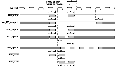 Figure 6-10 EMIFA Basic SDRAM Write Operation
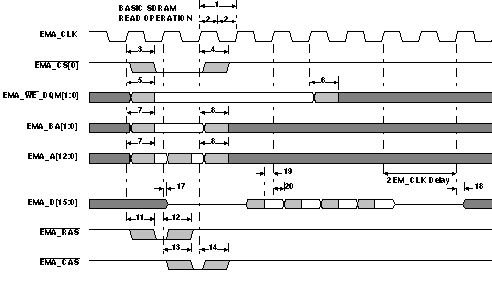 Figure 6-11 EMIFA Basic SDRAM Read Operation
Table 6-21 Timing Requirements for EMIFA Asynchronous Memory Interface (1)
| NO. | 1.2V | 1.1V | 1.0V | UNIT | |||||
|---|---|---|---|---|---|---|---|---|---|
| MIN | MAX | MIN | MAX | MIN | MAX | ||||
| READS and WRITES | |||||||||
| E | tc(CLK) | Cycle time, EMIFA module clock | 6.75 | 13.33 | 20 | ns | |||
| 2 | tw(EM_WAIT) | Pulse duration, EM_WAIT assertion and deassertion | 2E | 2E | 2E | ns | |||
| READS | |||||||||
| 12 | tsu(EMDV-EMOEH) | Setup time, EM_D[15:0] valid before EM_OE high | 3 | 5 | 7 | ns | |||
| 13 | th(EMOEH-EMDIV) | Hold time, EM_D[15:0] valid after EM_OE high | 0 | 0 | 0 | ns | |||
| 14 | tsu(EMOEL-EMWAIT) | Setup Time, EM_WAIT asserted before end of Strobe Phase(2) | 4E+3 | 4E+3 | 4E+3 | ns | |||
| WRITES | |||||||||
| 28 | tsu(EMWEL-EMWAIT) | Setup Time, EM_WAIT asserted before end of Strobe Phase(2) | 4E+3 | 4E+3 | 4E+3 | ns | |||
Table 6-22 Switching Characteristics for EMIFA Asynchronous Memory Interface(1)(2)(3)
| NO. | PARAMETER | 1.2V, 1.1V, 1.0V | UNIT | |||
|---|---|---|---|---|---|---|
| MIN | Nom | MAX | ||||
| READS and WRITES | ||||||
| 1 | td(TURNAROUND) | Turn around time | (TA)*E - 3 | (TA)*E | (TA)*E + 3 | ns |
| READS | ||||||
| 3 | tc(EMRCYCLE) | EMIF read cycle time (EW = 0) | (RS+RST+RH)*E - 3 | (RS+RST+RH)*E | (RS+RST+RH)*E + 3 | ns |
| EMIF read cycle time (EW = 1) | (RS+RST+RH+EWC)*E - 3 | (RS+RST+RH+EWC)*E | (RS+RST+RH+EWC)*E + 3 | ns | ||
| 4 | tsu(EMCEL-EMOEL) | Output setup time, EMA_CE[5:2] low to EMA_OE low (SS = 0) | (RS)*E-3 | (RS)*E | (RS)*E+3 | ns |
| Output setup time, EMA_CE[5:2] low to EMA_OE low (SS = 1) | -3 | 0 | +3 | ns | ||
| 5 | th(EMOEH-EMCEH) | Output hold time, EMA_OE high to EMA_CE[5:2] high (SS = 0) | (RH)*E - 3 | (RH)*E | (RH)*E + 3 | ns |
| Output hold time, EMA_OE high to EMA_CE[5:2] high (SS = 1) | -3 | 0 | +3 | ns | ||
| 6 | tsu(EMBAV-EMOEL) | Output setup time, EMA_BA[1:0] valid to EMA_OE low | (RS)*E-3 | (RS)*E | (RS)*E+3 | ns |
| 7 | th(EMOEH-EMBAIV) | Output hold time, EMA_OE high to EMA_BA[1:0] invalid | (RH)*E-3 | (RH)*E | (RH)*E+3 | ns |
| 8 | tsu(EMBAV-EMOEL) | Output setup time, EMA_A[13:0] valid to EMA_OE low | (RS)*E-3 | (RS)*E | (RS)*E+3 | ns |
| 9 | th(EMOEH-EMAIV) | Output hold time, EMA_OE high to EMA_A[13:0] invalid | (RH)*E-3 | (RH)*E | (RH)*E+3 | ns |
| 10 | tw(EMOEL) | EMA_OE active low width (EW = 0) | (RST)*E-3 | (RST)*E | (RST)*E+3 | ns |
| EMA_OE active low width (EW = 1) | (RST+EWC)*E-3 | (RST+EWC)*E | (RST+EWC)*E+3 | ns | ||
| 11 | td(EMWAITH-EMOEH) | Delay time from EMA_WAIT deasserted to EMA_OE high | 3E-3 | 4E | 4E+3 | ns |
| 28 | tsu(EMARW-EMOEL) | Output setup time, EMA_A_RW valid to EMA_OE low | (RS)*E-3 | (RS)*E | (RS)*E+3 | ns |
| 29 | th(EMOEH-EMARW) | Output hold time, EMA_OE high to EMA_A_RW invalid | (RH)*E-3 | (RH)*E | (RH)*E+3 | ns |
| WRITES | ||||||
| 15 | tc(EMWCYCLE) | EMIF write cycle time (EW = 0) | (WS+WST+WH)*E-3 | (WS+WST+WH)*E | (WS+WST+WH)*E+3 | ns |
| EMIF write cycle time (EW = 1) | (WS+WST+WH+EWC)*E - 3 | (WS+WST+WH+EWC)*E | (WS+WST+WH+EWC)*E + 3 | ns | ||
| 16 | tsu(EMCEL-EMWEL) | Output setup time, EMA_CE[5:2] low to EMA_WE low (SS = 0) | (WS)*E - 3 | (WS)*E | (WS)*E + 3 | ns |
| Output setup time, EMA_CE[5:2] low to EMA_WE low (SS = 1) | -3 | 0 | +3 | ns | ||
| 17 | th(EMWEH-EMCEH) | Output hold time, EMA_WE high to EMA_CE[5:2] high (SS = 0) | (WH)*E-3 | (WH)*E | (WH)*E+3 | ns |
| Output hold time, EMA_WE high to EMA_CE[5:2] high (SS = 1) | -3 | 0 | +3 | ns | ||
| 18 | tsu(EMDQMV-EMWEL) | Output setup time, EMA_BA[1:0] valid to EMA_WE low | (WS)*E-3 | (WS)*E | (WS)*E+3 | ns |
| 19 | th(EMWEH-EMDQMIV) | Output hold time, EMA_WE high to EMA_BA[1:0] invalid | (WH)*E-3 | (WH)*E | (WH)*E+3 | ns |
| 20 | tsu(EMBAV-EMWEL) | Output setup time, EMA_BA[1:0] valid to EMA_WE low | (WS)*E-3 | (WS)*E | (WS)*E+3 | ns |
| 21 | th(EMWEH-EMBAIV) | Output hold time, EMA_WE high to EMA_BA[1:0] invalid | (WH)*E-3 | (WH)*E | (WH)*E+3 | ns |
| 22 | tsu(EMAV-EMWEL) | Output setup time, EMA_A[13:0] valid to EMA_WE low | (WS)*E-3 | (WS)*E | (WS)*E+3 | ns |
| 23 | th(EMWEH-EMAIV) | Output hold time, EMA_WE high to EMA_A[13:0] invalid | (WH)*E-3 | (WH)*E | (WH)*E+3 | ns |
| 24 | tw(EMWEL) | EMA_WE active low width (EW = 0) | (WST)*E-3 | (WST)*E | (WST)*E+3 | ns |
| EMA_WE active low width (EW = 1) | (WST+EWC)*E-3 | (WST+EWC)*E | (WST+EWC)*E+3 | ns | ||
| 25 | td(EMWAITH-EMWEH) | Delay time from EMA_WAIT deasserted to EMA_WE high | 3E-3 | 4E | 4E+3 | ns |
| 26 | tsu(EMDV-EMWEL) | Output setup time, EMA_D[15:0] valid to EMA_WE low | (WS)*E-3 | (WS)*E | (WS)*E+3 | ns |
| 27 | th(EMWEH-EMDIV) | Output hold time, EMA_WE high to EMA_D[15:0] invalid | (WH)*E-3 | (WH)*E | (WH)*E+3 | ns |
| 30 | tsu(EMARW-EMWEL) | Output setup time, EMA_A_RW valid to EMA_WE low | (WS)*E-3 | (WS)*E | (WS)*E+3 | ns |
| 31 | th(EMWEH-EMARW) | Output hold time, EMA_WE high to EMA_A_RW invalid | (WH)*E-3 | (WH)*E | (WH)*E+3 | ns |
 Figure 6-12 Asynchronous Memory Read Timing for EMIFA
 Figure 6-13 Asynchronous Memory Write Timing for EMIFA
 Figure 6-14 EMA_WAIT Read Timing Requirements
 Figure 6-15 EMA_WAIT Write Timing Requirements
6.11 DDR2/mDDR Controller
The DDR2/mDDR Memory Controller is a dedicated interface to DDR2/mDDR SDRAM. It supports JESD79-2A standard compliant DDR2 SDRAM devices and compliant Mobile DDR SDRAM devices.
The DDR2/mDDR Memory Controller support the following features:
- JESD79-2A standard compliant DDR2 SDRAM
- Mobile DDR SDRAM
- 256-MB memory space for DDR2
- 256-MB memory space for mDDR
- CAS latencies:
- DDR2: 2, 3, 4 and 5
- mDDR: 2 and 3
- Internal banks:
- DDR2: 1, 2, 4 and 8
- mDDR:1, 2 and 4
- Burst length: 8
- Burst type: sequential
- 1 chip select (CS) signal
- Page sizes: 256, 512, 1024 and 2048
- SDRAM autoinitialization
- Self-refresh mode
- Partial array self-refresh (for mDDR)
- Power down mode
- Prioritized refresh
- Programmable refresh rate and backlog counter
- Programmable timing parameters
- Little endian
6.11.1 DDR2/mDDR Memory Controller Electrical Data/Timing
Table 6-23 Switching Characteristics Over Recommended Operating Conditions for DDR2/mDDR Memory Controller
| No. | PARAMETER | 1.2V | 1.1V | 1.0V | UNIT | |||||
|---|---|---|---|---|---|---|---|---|---|---|
| MIN | MAX | MIN | MAX | MIN | MAX | |||||
| 1 | tc(DDR_CLK) | Cycle time, DDR_CLKP / DDR_CLKN |
DDR2 | 125 | 156 | 125 | 150 | —(1) | —(1) | MHz |
| mDDR | 105 | 150 | 100 | 133 | 95 | 133 | ||||
6.11.2 DDR2/mDDR Controller Register Description(s)
Table 6-24 DDR2/mDDR Controller Registers
| BYTE ADDRESS | ACRONYM | REGISTER DESCRIPTION |
|---|---|---|
| 0xB000 0000 | REVID | Revision ID Register |
| 0xB000 0004 | SDRSTAT | SDRAM Status Register |
| 0xB000 0008 | SDCR | SDRAM Configuration Register |
| 0xB000 000C | SDRCR | SDRAM Refresh Control Register |
| 0xB000 0010 | SDTIMR1 | SDRAM Timing Register 1 |
| 0xB000 0014 | SDTIMR2 | SDRAM Timing Register 2 |
| 0xB000 001C | SDCR2 | SDRAM Configuration Register 2 |
| 0xB000 0020 | PBBPR | Peripheral Bus Burst Priority Register |
| 0xB000 0040 | PC1 | Performance Counter 1 Registers |
| 0xB000 0044 | PC2 | Performance Counter 2 Register |
| 0xB000 0048 | PCC | Performance Counter Configuration Register |
| 0xB000 004C | PCMRS | Performance Counter Master Region Select Register |
| 0xB000 0050 | PCT | Performance Counter Time Register |
| 0xB000 00C0 | IRR | Interrupt Raw Register |
| 0xB000 00C4 | IMR | Interrupt Mask Register |
| 0xB000 00C8 | IMSR | Interrupt Mask Set Register |
| 0xB000 00CC | IMCR | Interrupt Mask Clear Register |
| 0xB000 00E4 | DRPYC1R | DDR PHY Control Register 1 |
| 0x01E2 C000 | VTPIO_CTL | VTP IO Control Register |
6.11.3 DDR2/mDDR Interface
This section provides the timing specification for the DDR2/mDDR interface as a PCB design and manufacturing specification. The design rules constrain PCB trace length, PCB trace skew, signal integrity, cross-talk, and signal timing. These rules, when followed, result in a reliable DDR2/mDDR memory system without the need for a complex timing closure process. For more information regarding guidelines for using this DDR2/mDDR specification, Understanding TI's PCB Routing Rule-Based DDR2 Timing Specification (SPRAAV0).
6.11.3.1 DDR2/mDDR Interface Schematic
Figure 6-16 shows the DDR2/mDDR interface schematic for a single-memory DDR2/mDDR system. The dual-memory system shown in Figure 6-17. Pin numbers for the device can be obtained from the pin description section.
6.11.3.2 Compatible JEDEC DDR2/mDDR Devices
Table 6-25 shows the parameters of the JEDEC DDR2/mDDR devices that are compatible with this interface. Generally, the DDR2/mDDR interface is compatible with x16 DDR2-400/mDDR-200 speed grade DDR2/mDDR devices.
The device also supports JEDEC DDR2/mDDR x8 devices in the dual chip configuration. In this case, one chip supplies the upper byte and the second chip supplies the lower byte. Addresses and most control signals are shared just like regular dual chip memory configurations.
Table 6-25 Compatible JEDEC DDR2/mDDR Devices
| NO. | PARAMETER | MIN | MAX | UNIT |
|---|---|---|---|---|
| 1 | JEDEC DDR2/mDDR Device Speed Grade(1) | DDR2-400/mDDR-200 | ||
| 2 | JEDEC DDR2/mDDR Device Bit Width | x8 | x16 | Bits |
| 3 | JEDEC DDR2/mDDR Device Count(2) | 1 | 2 | Devices |
6.11.3.3 PCB Stackup
The minimum stackup required for routing the device is a six layer stack as shown in Table 6-26. Additional layers may be added to the PCB stack up to accommodate other circuitry or to reduce the size of the PCB footprint.Complete stack up specifications are provided in Table 6-27.
Table 6-26 Device Minimum PCB Stack Up
| LAYER | TYPE | DESCRIPTION |
|---|---|---|
| 1 | Signal | Top Routing Mostly Horizontal |
| 2 | Plane | Ground |
| 3 | Plane | Power |
| 4 | Signal | Internal Routing |
| 5 | Plane | Ground |
| 6 | Signal | Bottom Routing Mostly Vertical |
Table 6-27 PCB Stack Up Specifications
| NO. | PARAMETER | MIN | TYP | MAX | UNIT |
|---|---|---|---|---|---|
| 1 | PCB Routing/Plane Layers | 6 | |||
| 2 | Signal Routing Layers | 3 | |||
| 3 | Full ground layers under DDR2/mDDR routing region | 2 | |||
| 4 | Number of ground plane cuts allowed within DDR routing region | 0 | |||
| 5 | Number of ground reference planes required for each DDR2/mDDR routing layer | 1 | |||
| 6 | Number of layers between DDR2/mDDR routing layer and reference ground plane | 0 | |||
| 7 | PCB Routing Feature Size | 4 | Mils | ||
| 8 | PCB Trace Width w | 4 | Mils | ||
| 8 | PCB BGA escape via pad size | 18 | Mils | ||
| 9 | PCB BGA escape via hole size | 8 | Mils | ||
| 10 | Device BGA pad size(1) | ||||
| 11 | DDR2/mDDR Device BGA pad size(2) | ||||
| 12 | Single Ended Impedance, Zo | 50 | 75 | Ω | |
| 13 | Impedance Control(3) | Z-5 | Z | Z+5 | Ω |
6.11.3.4 Placement
Figure 6-17 shows the required placement for the device as well as the DDR2/mDDR devices. The dimensions for Figure 6-18 are defined in Table 6-28. The placement does not restrict the side of the PCB that the devices are mounted on. The ultimate purpose of the placement is to limit the maximum trace lengths and allow for proper routing space. For single-memory DDR2/mDDR systems, the second DDR2/mDDR device is omitted from the placement.
 Figure 6-18 Device and DDR2/mDDR Device Placement
Table 6-28 Placement Specifications(1)(2)
| NO. | PARAMETER | MIN | MAX | UNIT |
|---|---|---|---|---|
| 1 | X | 1750 | Mils | |
| 2 | Y | 1280 | Mils | |
| 3 | Y Offset | (3) | 650 | Mils |
| 4 | Clearance from non-DDR2/mDDR signal to DDR2/mDDR Keepout Region(4) | 4 | w(5) |
6.11.3.5 DDR2/mDDR Keep Out Region
The region of the PCB used for the DDR2/mDDR circuitry must be isolated from other signals. The DDR2/mDDR keep out region is defined for this purpose and is shown in Figure 6-19. The size of this region varies with the placement and DDR routing. Additional clearances required for the keep out region are shown in Table 6-28.
 Figure 6-19 DDR2/mDDR Keepout Region
6.11.3.6 Bulk Bypass Capacitors
Bulk bypass capacitors are required for moderate speed bypassing of the DDR2/mDDR and other circuitry. Table 6-29 contains the minimum numbers and capacitance required for the bulk bypass capacitors. Note that this table only covers the bypass needs of the device and DDR2/mDDR interfaces. Additional bulk bypass capacitance may be needed for other circuitry.
Table 6-29 Bulk Bypass Capacitors
| NO. | PARAMETER | MIN | MAX | UNIT |
|---|---|---|---|---|
| 1 | DDR_DVDD18 Supply Bulk Bypass Capacitor Count(1) | 3 | Devices | |
| 2 | DDR_DVDD18 Supply Bulk Bypass Total Capacitance | 30 | μF | |
| 3 | DDR#1 Bulk Bypass Capacitor Count(1) | 1 | Devices | |
| 4 | DDR#1 Bulk Bypass Total Capacitance | 22 | μF | |
| 5 | DDR#2 Bulk Bypass Capacitor Count(1)(2) | 1 | Devices | |
| 6 | DDR#2 Bulk Bypass Total Capacitance(2) | 22 | μF |
6.11.3.7 High-Speed Bypass Capacitors
High-speed (HS) bypass capacitors are critical for proper DDR2/mDDR interface operation. It is particularly important to minimize the parasitic series inductance of the HS bypass cap, device/DDR2/mDDR power, and device/DDR2/mDDR ground connections. Table 6-30 contains the specification for the HS bypass capacitors as well as for the power connections on the PCB.
Table 6-30 High-Speed Bypass Capacitors
| NO. | PARAMETER | MIN | MAX | UNIT |
|---|---|---|---|---|
| 1 | HS Bypass Capacitor Package Size(1) | 0402 | 10 Mils | |
| 2 | Distance from HS bypass capacitor to device being bypassed | 250 | Mils | |
| 3 | Number of connection vias for each HS bypass capacitor | 2(4) | Vias | |
| 4 | Trace length from bypass capacitor contact to connection via | 1 | 30 | Mils |
| 5 | Number of connection vias for each DDR2/mDDR device power or ground balls | 1 | Vias | |
| 6 | Trace length from DDR2/mDDR device power ball to connection via | 35 | Mils | |
| 7 | DDR_DVDD18 Supply HS Bypass Capacitor Count(2) | 10 | Devices | |
| 8 | DDR_DVDD18 Supply HS Bypass Capacitor Total Capacitance | 0.6 | μF | |
| 9 | DDR#1 HS Bypass Capacitor Count(2) | 8 | Devices | |
| 10 | DDR#1 HS Bypass Capacitor Total Capacitance | 0.4 | μF | |
| 11 | DDR#2 HS Bypass Capacitor Count(2)(3) | 8 | Devices | |
| 12 | DDR#2 HS Bypass Capacitor Total Capacitance(3) | 0.4 | μF |
6.11.3.8 Net Classes
Table 6-31 lists the clock net classes for the DDR2/mDDR interface. Table 6-32 lists the signal net classes, and associated clock net classes, for the signals in the DDR2/mDDR interface. These net classes are used for the termination and routing rules that follow.
Table 6-31 Clock Net Class Definitions
| CLOCK NET CLASS | PIN NAMES |
|---|---|
| CK | DDR_CLKP / DDR_CLKN |
| DQS0 | DDR_DQS[0] |
| DQS1 | DDR_DQS[1] |
Table 6-32 Signal Net Class Definitions
| SIGNAL NET CLASS | ASSOCIATED CLOCK NET CLASS | PIN NAMES |
|---|---|---|
| ADDR_CTRL | CK | DDR_BA[2:0], DDR_A[13:0], DDR_CS, DDR_CAS, DDR_RAS, DDR_WE, DDR_CKE |
| D0 | DQS0 | DDR_D[7:0], DDR_DQM0 |
| D1 | DQS1 | DDR_D[15:8], DDR_DQM1 |
| DQGATE | CK, DQS0, DQS1 | DDR_DQGATE0, DDR_DQGATE1 |
6.11.3.9 DDR2/mDDR Signal Termination
No terminations of any kind are required in order to meet signal integrity and overshoot requirements. Serial terminators are permitted, if desired, to reduce EMI risk; however, serial terminations are the only type permitted. Table 6-33 shows the specifications for the series terminators.
Table 6-33 DDR2/mDDR Signal Terminations(1)(2)(3)
| NO. | PARAMETER | MIN | TYP | MAX | UNIT |
|---|---|---|---|---|---|
| 1 | CK Net Class | 0 | 10 | Ω | |
| 2 | ADDR_CTRL Net Class | 0 | 22 | Zo | Ω |
| 3 | Data Byte Net Classes (DQS[0], DQS[1], D0, D1)(4) | 0 | 22 | Zo | Ω |
| 4 | DQGATE Net Class (DQGATE) | 0 | 10 | Zo | Ω |
6.11.3.10 VREF Routing
VREF is used as a reference by the input buffers of the DDR2/mDDR memories as well as the device. VREF is intended to be half the DDR2/mDDR power supply voltage and should be created using a resistive divider as shown in Figure 6-16. Other methods of creating VREF are not recommended. Figure 6-20 shows the layout guidelines for VREF.
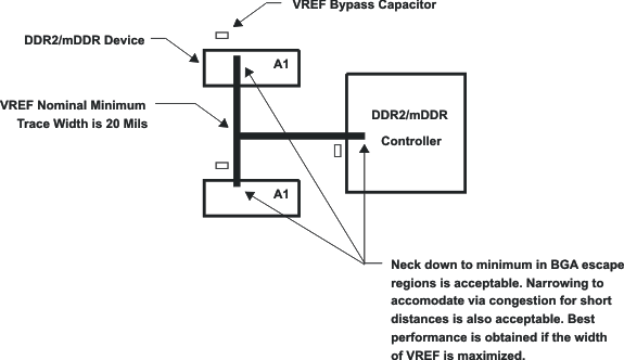 Figure 6-20 VREF Routing and Topology
6.11.3.11 DDR2/mDDR CK and ADDR_CTRL Routing
Figure 6-21 shows the topology of the routing for the CK and ADDR_CTRL net classes. The route is a balanced T as it is intended that the length of segments B and C be equal. In addition, the length of A should be maximized.
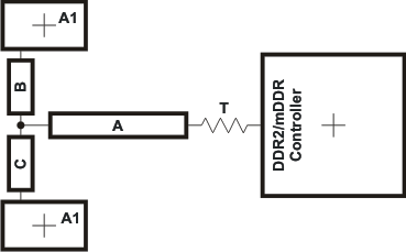 Figure 6-21 CK and ADDR_CTRL Routing and Topology
Table 6-34 CK and ADDR_CTRL Routing Specification
| NO. | PARAMETER | MIN | TYP | MAX | UNIT |
|---|---|---|---|---|---|
| 1 | Center to Center CK-CKN Spacing(3) | 2w(4) | |||
| 2 | CK A to B/A to C Skew Length Mismatch(1) | 25 | Mils | ||
| 3 | CK B to C Skew Length Mismatch | 25 | Mils | ||
| 4 | Center to center CK to other DDR2/mDDR trace spacing(3) | 4w(4) | |||
| 5 | CK/ADDR_CTRL nominal trace length(2) | CACLM-50 | CACLM | CACLM+50 | Mils |
| 6 | ADDR_CTRL to CK Skew Length Mismatch | 100 | Mils | ||
| 7 | ADDR_CTRL to ADDR_CTRL Skew Length Mismatch | 100 | Mils | ||
| 8 | Center to center ADDR_CTRL to other DDR2/mDDR trace spacing(3) | 4w(4) | |||
| 9 | Center to center ADDR_CTRL to other ADDR_CTRL trace spacing(3) | 3w (4) | |||
| 10 | ADDR_CTRL A to B/A to C Skew Length Mismatch(1) | 100 | Mils | ||
| 11 | ADDR_CTRL B to C Skew Length Mismatch | 100 | Mils |
Figure 6-22 shows the topology and routing for the DQS and D net class; the routes are point to point. Skew matching across bytes is not needed nor recommended.
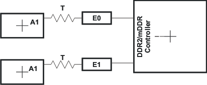 Figure 6-22 DQS and D Routing and Topology
Table 6-35 DQS and D Routing Specification
| NO. | PARAMETER | MIN | TYP | MAX | UNIT |
|---|---|---|---|---|---|
| 1 | Center to center DQS to other DDR2/mDDR trace spacing(4) | 4w(6) | |||
| 2 | DQS/D nominal trace length(1)(3) | DQLM-50 | DQLM | DQLM+50 | Mils |
| 3 | D to DQS Skew Length Mismatch(3) | 100 | Mils | ||
| 4 | D to D Skew Length Mismatch(3) | 100 | Mils | ||
| 5 | Center to center D to other DDR2/mDDR trace spacing(4)(5) | 4w(6) | |||
| 6 | Center to Center D to other D trace spacing(4)(2) | 3w(6) |
Figure 6-23 shows the routing for the DQGATE net class. Table 6-36 contains the routing specification.
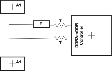 Figure 6-23 DQGATE Routing
Table 6-36 DQGATE Routing Specification
| NO. | PARAMETER | MIN | TYP | MAX | UNIT |
|---|---|---|---|---|---|
| 1 | DQGATE Length F | CKB0B(1) | |||
| 2 | Center to center DQGATE to any other trace spacing | 4w(3) | |||
| 3 | DQS/D nominal trace length | DQLM-50 | DQLM | DQLM+50 | Mils |
| 4 | DQGATE Skew(2) | 100 | Mils |
6.11.3.12 MDDR/DDR2 Boundary Scan Limitations
Due to DDR implementation and timing restrictions, it was not possible to place boundary scan cells between core logic and the IO like boundary scan cells for other IO. Instead, the boundary scan cells are tapped-off to the DDR PHY and there is the equivalent of a multiplexer inside the DDR PHY which selects between functional and boundary scan paths.
The implication for boundary scan is that the DDR pins will not support the SAMPLE function of the output enable cells on the DDR pins and this is a violation of IEEE 1149.1. Full EXTEST and PRELOAD capability is still available.
6.12 Memory Protection Units
The MPU performs memory protection checking. It receives requests from a bus master in the system and checks the address against the fixed and programmable regions to see if the access is allowed. If allowed, the transfer is passed unmodified to its output bus (to the targeted address). If the transfer is illegal (fails the protection check) then the MPU does not pass the transfer to the output bus but rather services the transfer internally back to the input bus (to prevent a hang) returning the fault status to the requestor as well as generating an interrupt about the fault. The following features are supported by the MPU:
- Provides memory protection for fixed and programmable address ranges.
- Supports multiple programmable address region.
- Supports secure and debug access privileges.
- Supports read, write, and execute access privileges.
- Supports privid(8) associations with ranges.
- Generates an interrupt when there is a protection violation, and saves violating transfer parameters.
- MMR access is also protected.
Table 6-37 MPU1 Configuration Registers
| MPU1 BYTE ADDRESS |
ACRONYM | REGISTER DESCRIPTION |
|---|---|---|
| 0x01E1 4000 | REVID | Revision ID |
| 0x01E1 4004 | CONFIG | Configuration |
| 0x01E1 4010 | IRAWSTAT | Interrupt raw status/set |
| 0x01E1 4014 | IENSTAT | Interrupt enable status/clear |
| 0x01E1 4018 | IENSET | Interrupt enable |
| 0x01E1 401C | IENCLR | Interrupt enable clear |
| 0x01E1 4020 - 0x01E1 41FF | - | Reserved |
| 0x01E1 4200 | PROG1_MPSAR | Programmable range 1, start address |
| 0x01E1 4204 | PROG1_MPEAR | Programmable range 1, end address |
| 0x01E1 4208 | PROG1_MPPA | Programmable range 1, memory page protection attributes |
| 0x01E1 420C - 0x01E1 420F | - | Reserved |
| 0x01E1 4210 | PROG2_MPSAR | Programmable range 2, start address |
| 0x01E1 4214 | PROG2_MPEAR | Programmable range 2, end address |
| 0x01E1 4218 | PROG2_MPPA | Programmable range 2, memory page protection attributes |
| 0x01E1 421C - 0x01E1 421F | - | Reserved |
| 0x01E1 4220 | PROG3_MPSAR | Programmable range 3, start address |
| 0x01E1 4224 | PROG3_MPEAR | Programmable range 3, end address |
| 0x01E1 4228 | PROG3_MPPA | Programmable range 3, memory page protection attributes |
| 0x01E1 422C - 0x01E1 422F | - | Reserved |
| 0x01E1 4230 | PROG4_MPSAR | Programmable range 4, start address |
| 0x01E1 4234 | PROG4_MPEAR | Programmable range 4, end address |
| 0x01E1 4238 | PROG4_MPPA | Programmable range 4, memory page protection attributes |
| 0x01E1 423C - 0x01E1 423F | - | Reserved |
| 0x01E1 4240 | PROG5_MPSAR | Programmable range 5, start address |
| 0x01E1 4244 | PROG5_MPEAR | Programmable range 5, end address |
| 0x01E1 4248 | PROG5_MPPA | Programmable range 5, memory page protection attributes |
| 0x01E1 424C - 0x01E1 424F | - | Reserved |
| 0x01E1 4250 | PROG6_MPSAR | Programmable range 6, start address |
| 0x01E1 4254 | PROG6_MPEAR | Programmable range 6, end address |
| 0x01E1 4258 | PROG6_MPPA | Programmable range 6, memory page protection attributes |
| 0x01E1 425C - 0x01E1 42FF | - | Reserved |
| 0x01E1 4300 | FLTADDRR | Fault address |
| 0x01E1 4304 | FLTSTAT | Fault status |
| 0x01E1 4308 | FLTCLR | Fault clear |
| 0x01E1 430C - 0x01E1 4FFF | - | Reserved |
Table 6-38 MPU2 Configuration Registers
| MPU2 BYTE ADDRESS |
ACRONYM | REGISTER DESCRIPTION |
|---|---|---|
| 0x01E1 5000 | REVID | Revision ID |
| 0x01E1 5004 | CONFIG | Configuration |
| 0x01E1 5010 | IRAWSTAT | Interrupt raw status/set |
| 0x01E1 5014 | IENSTAT | Interrupt enable status/clear |
| 0x01E1 5018 | IENSET | Interrupt enable |
| 0x01E1 501C | IENCLR | Interrupt enable clear |
| 0x01E1 5020 - 0x01E1 51FF | - | Reserved |
| 0x01E1 5200 | PROG1_MPSAR | Programmable range 1, start address |
| 0x01E1 5204 | PROG1_MPEAR | Programmable range 1, end address |
| 0x01E1 5208 | PROG1_MPPA | Programmable range 1, memory page protection attributes |
| 0x01E1 520C - 0x01E1 520F | - | Reserved |
| 0x01E1 5210 | PROG2_MPSAR | Programmable range 2, start address |
| 0x01E1 5214 | PROG2_MPEAR | Programmable range 2, end address |
| 0x01E1 5218 | PROG2_MPPA | Programmable range 2, memory page protection attributes |
| 0x01E1 521C - 0x01E1 521F | - | Reserved |
| 0x01E1 5220 | PROG3_MPSAR | Programmable range 3, start address |
| 0x01E1 5224 | PROG3_MPEAR | Programmable range 3, end address |
| 0x01E1 5228 | PROG3_MPPA | Programmable range 3, memory page protection attributes |
| 0x01E1 522C - 0x01E1 522F | - | Reserved |
| 0x01E1 5230 | PROG4_MPSAR | Programmable range 4, start address |
| 0x01E1 5234 | PROG4_MPEAR | Programmable range 4, end address |
| 0x01E1 5238 | PROG4_MPPA | Programmable range 4, memory page protection attributes |
| 0x01E1 523C - 0x01E1 523F | - | Reserved |
| 0x01E1 5240 | PROG5_MPSAR | Programmable range 5, start address |
| 0x01E1 5244 | PROG5_MPEAR | Programmable range 5, end address |
| 0x01E1 5248 | PROG5_MPPA | Programmable range 5, memory page protection attributes |
| 0x01E1 524C - 0x01E1 524F | - | Reserved |
| 0x01E1 5250 | PROG6_MPSAR | Programmable range 6, start address |
| 0x01E1 5254 | PROG6_MPEAR | Programmable range 6, end address |
| 0x01E1 5258 | PROG6_MPPA | Programmable range 6, memory page protection attributes |
| 0x01E1 525C - 0x01E1 525F | - | Reserved |
| 0x01E1 5260 | PROG7_MPSAR | Programmable range 7, start address |
| 0x01E1 5264 | PROG7_MPEAR | Programmable range 7, end address |
| 0x01E1 5268 | PROG7_MPPA | Programmable range 7, memory page protection attributes |
| 0x01E1 526C - 0x01E1 526F | - | Reserved |
| 0x01E1 5270 | PROG8_MPSAR | Programmable range 8, start address |
| 0x01E1 5274 | PROG8_MPEAR | Programmable range 8, end address |
| 0x01E1 5278 | PROG8_MPPA | Programmable range 8, memory page protection attributes |
| 0x01E1 527C - 0x01E1 527F | - | Reserved |
| 0x01E1 5280 | PROG9_MPSAR | Programmable range 9, start address |
| 0x01E1 5284 | PROG9_MPEAR | Programmable range 9, end address |
| 0x01E1 5288 | PROG9_MPPA | Programmable range 9, memory page protection attributes |
| 0x01E1 528C - 0x01E1 528F | - | Reserved |
| 0x01E1 5290 | PROG10_MPSAR | Programmable range 10, start address |
| 0x01E1 5294 | PROG10_MPEAR | Programmable range 10, end address |
| 0x01E1 5298 | PROG10_MPPA | Programmable range 10, memory page protection attributes |
| 0x01E1 529C - 0x01E1 529F | - | Reserved |
| 0x01E1 52A0 | PROG11_MPSAR | Programmable range 11, start address |
| 0x01E1 52A4 | PROG11_MPEAR | Programmable range 11, end address |
| 0x01E1 52A8 | PROG11_MPPA | Programmable range 11, memory page protection attributes |
| 0x01E1 52AC - 0x01E1 52AF | - | Reserved |
| 0x01E1 52B0 | PROG12_MPSAR | Programmable range 12, start address |
| 0x01E1 52B4 | PROG12_MPEAR | Programmable range 12, end address |
| 0x01E1 52B8 | PROG12_MPPA | Programmable range 12, memory page protection attributes |
| 0x01E1 52BC - 0x01E1 52FF | - | Reserved |
| 0x01E1 5300 | FLTADDRR | Fault address |
| 0x01E1 5304 | FLTSTAT | Fault status |
| 0x01E1 5308 | FLTCLR | Fault clear |
| 0x01E1 530C - 0x01E1 5FFF | - | Reserved |
6.13 MMC / SD / SDIO (MMCSD0)
6.13.1 MMCSD Peripheral Description
The device includes one MMCSD controller which is compliant with MMC V4.0, Secure Digital Part 1 Physical Layer Specification V1.1 and Secure Digital Input Output (SDIO) V2.0 specifications.
The MMC/SD Controller has following features:
- MultiMediaCard (MMC)
- Secure Digital (SD) Memory Card
- MMC/SD protocol support
- SD high capacity support
- SDIO protocol support
- Programmable clock frequency
- 512 bit Read/Write FIFO to lower system overhead
- Slave EDMA transfer capability
The device MMC/SD Controller does not support SPI mode.
6.13.2 MMCSD Peripheral Register Description(s)
Table 6-39 Multimedia Card/Secure Digital (MMC/SD) Card Controller Registers
| MMCSD0 BYTE ADDRESS |
ACRONYM | REGISTER DESCSRIPTION |
|---|---|---|
| 0x01C4 0000 | MMCCTL | MMC Control Register |
| 0x01C4 0004 | MMCCLK | MMC Memory Clock Control Register |
| 0x01C4 0008 | MMCST0 | MMC Status Register 0 |
| 0x01C4 000C | MMCST1 | MMC Status Register 1 |
| 0x01C4 0010 | MMCIM | MMC Interrupt Mask Register |
| 0x01C4 0014 | MMCTOR | MMC Response Time-Out Register |
| 0x01C4 0018 | MMCTOD | MMC Data Read Time-Out Register |
| 0x01C4 001C | MMCBLEN | MMC Block Length Register |
| 0x01C4 0020 | MMCNBLK | MMC Number of Blocks Register |
| 0x01C4 0024 | MMCNBLC | MMC Number of Blocks Counter Register |
| 0x01C4 0028 | MMCDRR | MMC Data Receive Register |
| 0x01C4 002C | MMCDXR | MMC Data Transmit Register |
| 0x01C4 0030 | MMCCMD | MMC Command Register |
| 0x01C4 0034 | MMCARGHL | MMC Argument Register |
| 0x01C4 0038 | MMCRSP01 | MMC Response Register 0 and 1 |
| 0x01C4 003C | MMCRSP23 | MMC Response Register 2 and 3 |
| 0x01C4 0040 | MMCRSP45 | MMC Response Register 4 and 5 |
| 0x01C4 0044 | MMCRSP67 | MMC Response Register 6 and 7 |
| 0x01C4 0048 | MMCDRSP | MMC Data Response Register |
| 0x01C4 0050 | MMCCIDX | MMC Command Index Register |
| 0x01C4 0064 | SDIOCTL | SDIO Control Register |
| 0x01C4 0068 | SDIOST0 | SDIO Status Register 0 |
| 0x01C4 006C | SDIOIEN | SDIO Interrupt Enable Register |
| 0x01C4 0070 | SDIOIST | SDIO Interrupt Status Register |
| 0x01C4 0074 | MMCFIFOCTL | MMC FIFO Control Register |
6.13.3 MMC/SD Electrical Data/Timing
Table 6-40 through Table 6-41 assume testing over recommended operating conditions.
Table 6-40 Timing Requirements for MMC/SD
(see Figure 6-25 and Figure 6-27)
| NO. | 1.2V | 1.1V | 1.0V | UNIT | |||||
|---|---|---|---|---|---|---|---|---|---|
| MIN | MAX | MIN | MAX | MIN | MAX | ||||
| 1 | tsu(CMDV-CLKH) | Setup time, MMCSD_CMD valid before MMCSD_CLK high | 4 | 4 | 6 | ns | |||
| 2 | th(CLKH-CMDV) | Hold time, MMCSD_CMD valid after MMCSD_CLK high | 2.5 | 2.5 | 2.5 | ns | |||
| 3 | tsu(DATV-CLKH) | Setup time, MMCSD_DATx valid before MMCSD_CLK high | 4.5 | 5 | 6 | ns | |||
| 4 | th(CLKH-DATV) | Hold time, MMCSD_DATx valid after MMCSD_CLK high | 2.5 | 2.5 | 2.5 | ns | |||
Table 6-41 Switching Characteristics for MMC/SD (see Figure 6-24 through Figure 6-27)
| NO. | PARAMETER | 1.2V | 1.1V | 1.0V | UNIT | ||||
|---|---|---|---|---|---|---|---|---|---|
| MIN | MAX | MIN | MAX | MIN | MAX | ||||
| 7 | f(CLK) | Operating frequency, MMCSD_CLK | 0 | 52 | 0 | 50 | 0 | 25 | MHz |
| 8 | f(CLK_ID) | Identification mode frequency, MMCSD_CLK | 0 | 400 | 0 | 400 | 0 | 400 | KHz |
| 9 | tW(CLKL) | Pulse width, MMCSD_CLK low | 6.5 | 6.5 | 10 | ns | |||
| 10 | tW(CLKH) | Pulse width, MMCSD_CLK high | 6.5 | 6.5 | 10 | ns | |||
| 11 | tr(CLK) | Rise time, MMCSD_CLK | 3 | 3 | 10 | ns | |||
| 12 | tf(CLK) | Fall time, MMCSD_CLK | 3 | 3 | 10 | ns | |||
| 13 | td(CLKL-CMD) | Delay time, MMCSD_CLK low to MMCSD_CMD transition | -4 | 2.5 | -4 | 3 | -4 | 4 | ns |
| 14 | td(CLKL-DAT) | Delay time, MMCSD_CLK low to MMCSD_DATx transition | -4 | 3.3 | -4 | 3.5 | -4 | 4 | ns |
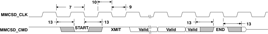 Figure 6-24 MMC/SD Host Command Timing
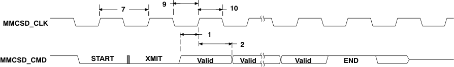 Figure 6-25 MMC/SD Card Response Timing
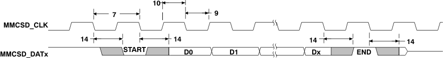 Figure 6-26 MMC/SD Host Write Timing
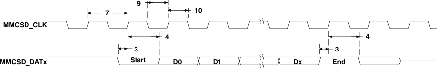 Figure 6-27 MMC/SD Host Read and Card CRC Status Timing
6.14 Multichannel Audio Serial Port (McASP)
The McASP serial port is specifically designed for multichannel audio applications. Its key features are:
- Flexible clock and frame sync generation logic and on-chip dividers
- Up to sixteen transmit or receive data pins and serializers
- Large number of serial data format options, including:
- TDM Frames with 2 to 32 time slots per frame (periodic) or 1 slot per frame (burst)
- Time slots of 8,12,16, 20, 24, 28, and 32 bits
- First bit delay 0, 1, or 2 clocks
- MSB or LSB first bit order
- Left- or right-aligned data words within time slots
- DIT Mode with 384-bit Channel Status and 384-bit User Data registers
- Extensive error checking and mute generation logic
- All unused pins GPIO-capable
- Transmit & Receive FIFO Buffers allow the McASP to operate at a higher sample rate by making it more tolerant to DMA latency.
- Dynamic Adjustment of Clock Dividers
- Clock Divider Value may be changed without resetting the McASP
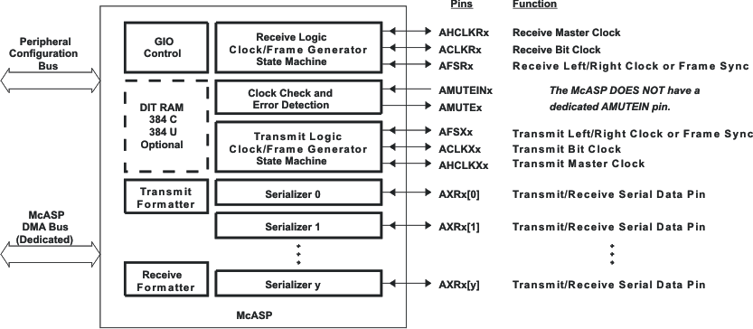 Figure 6-28 McASP Block Diagram
6.14.1 McASP Peripheral Registers Description(s)
Registers for the McASP are summarized in Table 6-42. The registers are accessed through the peripheral configuration port. The receive buffer registers (RBUF) and transmit buffer registers (XBUF) can also be accessed through the DMA port, as listed in Table 6-43
Registers for the McASP Audio FIFO (AFIFO) are summarized in Table 6-44. Note that the AFIFO Write FIFO (WFIFO) and Read FIFO (RFIFO) have independent control and status registers. The AFIFO control registers are accessed through the peripheral configuration port.
Table 6-42 McASP Registers Accessed Through Peripheral Configuration Port
| BYTE ADDRESS | ACRONYM | REGISTER DESCRIPTION |
|---|---|---|
| 0x01D0 0000 | REV | Revision identification register |
| 0x01D0 0010 | PFUNC | Pin function register |
| 0x01D0 0014 | PDIR | Pin direction register |
| 0x01D0 0018 | PDOUT | Pin data output register |
| 0x01D0 001C | PDIN | Read returns: Pin data input register |
| 0x01D0 001C | PDSET | Writes affect: Pin data set register (alternate write address: PDOUT) |
| 0x01D0 0020 | PDCLR | Pin data clear register (alternate write address: PDOUT) |
| 0x01D0 0044 | GBLCTL | Global control register |
| 0x01D0 0048 | AMUTE | Audio mute control register |
| 0x01D0 004C | DLBCTL | Digital loopback control register |
| 0x01D0 0050 | DITCTL | DIT mode control register |
| 0x01D0 0060 | RGBLCTL | Receiver global control register: Alias of GBLCTL, only receive bits are affected - allows receiver to be reset independently from transmitter |
| 0x01D0 0064 | RMASK | Receive format unit bit mask register |
| 0x01D0 0068 | RFMT | Receive bit stream format register |
| 0x01D0 006C | AFSRCTL | Receive frame sync control register |
| 0x01D0 0070 | ACLKRCTL | Receive clock control register |
| 0x01D0 0074 | AHCLKRCTL | Receive high-frequency clock control register |
| 0x01D0 0078 | RTDM | Receive TDM time slot 0-31 register |
| 0x01D0 007C | RINTCTL | Receiver interrupt control register |
| 0x01D0 0080 | RSTAT | Receiver status register |
| 0x01D0 0084 | RSLOT | Current receive TDM time slot register |
| 0x01D0 0088 | RCLKCHK | Receive clock check control register |
| 0x01D0 008C | REVTCTL | Receiver DMA event control register |
| 0x01D0 00A0 | XGBLCTL | Transmitter global control register. Alias of GBLCTL, only transmit bits are affected - allows transmitter to be reset independently from receiver |
| 0x01D0 00A4 | XMASK | Transmit format unit bit mask register |
| 0x01D0 00A8 | XFMT | Transmit bit stream format register |
| 0x01D0 00AC | AFSXCTL | Transmit frame sync control register |
| 0x01D0 00B0 | ACLKXCTL | Transmit clock control register |
| 0x01D0 00B4 | AHCLKXCTL | Transmit high-frequency clock control register |
| 0x01D0 00B8 | XTDM | Transmit TDM time slot 0-31 register |
| 0x01D0 00BC | XINTCTL | Transmitter interrupt control register |
| 0x01D0 00C0 | XSTAT | Transmitter status register |
| 0x01D0 00C4 | XSLOT | Current transmit TDM time slot register |
| 0x01D0 00C8 | XCLKCHK | Transmit clock check control register |
| 0x01D0 00CC | XEVTCTL | Transmitter DMA event control register |
| 0x01D0 0100 | DITCSRA0 | Left (even TDM time slot) channel status register (DIT mode) 0 |
| 0x01D0 0104 | DITCSRA1 | Left (even TDM time slot) channel status register (DIT mode) 1 |
| 0x01D0 0108 | DITCSRA2 | Left (even TDM time slot) channel status register (DIT mode) 2 |
| 0x01D0 010C | DITCSRA3 | Left (even TDM time slot) channel status register (DIT mode) 3 |
| 0x01D0 0110 | DITCSRA4 | Left (even TDM time slot) channel status register (DIT mode) 4 |
| 0x01D0 0114 | DITCSRA5 | Left (even TDM time slot) channel status register (DIT mode) 5 |
| 0x01D0 0118 | DITCSRB0 | Right (odd TDM time slot) channel status register (DIT mode) 0 |
| 0x01D0 011C | DITCSRB1 | Right (odd TDM time slot) channel status register (DIT mode) 1 |
| 0x01D0 0120 | DITCSRB2 | Right (odd TDM time slot) channel status register (DIT mode) 2 |
| 0x01D0 0124 | DITCSRB3 | Right (odd TDM time slot) channel status register (DIT mode) 3 |
| 0x01D0 0128 | DITCSRB4 | Right (odd TDM time slot) channel status register (DIT mode) 4 |
| 0x01D0 012C | DITCSRB5 | Right (odd TDM time slot) channel status register (DIT mode) 5 |
| 0x01D0 0130 | DITUDRA0 | Left (even TDM time slot) channel user data register (DIT mode) 0 |
| 0x01D0 0134 | DITUDRA1 | Left (even TDM time slot) channel user data register (DIT mode) 1 |
| 0x01D0 0138 | DITUDRA2 | Left (even TDM time slot) channel user data register (DIT mode) 2 |
| 0x01D0 013C | DITUDRA3 | Left (even TDM time slot) channel user data register (DIT mode) 3 |
| 0x01D0 0140 | DITUDRA4 | Left (even TDM time slot) channel user data register (DIT mode) 4 |
| 0x01D0 0144 | DITUDRA5 | Left (even TDM time slot) channel user data register (DIT mode) 5 |
| 0x01D0 0148 | DITUDRB0 | Right (odd TDM time slot) channel user data register (DIT mode) 0 |
| 0x01D0 014C | DITUDRB1 | Right (odd TDM time slot) channel user data register (DIT mode) 1 |
| 0x01D0 0150 | DITUDRB2 | Right (odd TDM time slot) channel user data register (DIT mode) 2 |
| 0x01D0 0154 | DITUDRB3 | Right (odd TDM time slot) channel user data register (DIT mode) 3 |
| 0x01D0 0158 | DITUDRB4 | Right (odd TDM time slot) channel user data register (DIT mode) 4 |
| 0x01D0 015C | DITUDRB5 | Right (odd TDM time slot) channel user data register (DIT mode) 5 |
| 0x01D0 0180 | SRCTL0 | Serializer control register 0 |
| 0x01D0 0184 | SRCTL1 | Serializer control register 1 |
| 0x01D0 0188 | SRCTL2 | Serializer control register 2 |
| 0x01D0 018C | SRCTL3 | Serializer control register 3 |
| 0x01D0 0190 | SRCTL4 | Serializer control register 4 |
| 0x01D0 0194 | SRCTL5 | Serializer control register 5 |
| 0x01D0 0198 | SRCTL6 | Serializer control register 6 |
| 0x01D0 019C | SRCTL7 | Serializer control register 7 |
| 0x01D0 01A0 | SRCTL8 | Serializer control register 8 |
| 0x01D0 01A4 | SRCTL9 | Serializer control register 9 |
| 0x01D0 01A8 | SRCTL10 | Serializer control register 10 |
| 0x01D0 01AC | SRCTL11 | Serializer control register 11 |
| 0x01D0 01B0 | SRCTL12 | Serializer control register 12 |
| 0x01D0 01B4 | SRCTL13 | Serializer control register 13 |
| 0x01D0 01B8 | SRCTL14 | Serializer control register 14 |
| 0x01D0 01BC | SRCTL15 | Serializer control register 15 |
| 0x01D0 0200 | XBUF0(1) | Transmit buffer register for serializer 0 |
| 0x01D0 0204 | XBUF1(1) | Transmit buffer register for serializer 1 |
| 0x01D0 0208 | XBUF2(1) | Transmit buffer register for serializer 2 |
| 0x01D0 020C | XBUF3(1) | Transmit buffer register for serializer 3 |
| 0x01D0 0210 | XBUF4(1) | Transmit buffer register for serializer 4 |
| 0x01D0 0214 | XBUF5(1) | Transmit buffer register for serializer 5 |
| 0x01D0 0218 | XBUF6(1) | Transmit buffer register for serializer 6 |
| 0x01D0 021C | XBUF7(1) | Transmit buffer register for serializer 7 |
| 0x01D0 0220 | XBUF8(1) | Transmit buffer register for serializer 8 |
| 0x01D0 0224 | XBUF9(1) | Transmit buffer register for serializer 9 |
| 0x01D0 0228 | XBUF10(1) | Transmit buffer register for serializer 10 |
| 0x01D0 022C | XBUF11(1) | Transmit buffer register for serializer 11 |
| 0x01D0 0230 | XBUF12(1) | Transmit buffer register for serializer 12 |
| 0x01D0 0234 | XBUF13(1) | Transmit buffer register for serializer 13 |
| 0x01D0 0238 | XBUF14(1) | Transmit buffer register for serializer 14 |
| 0x01D0 023C | XBUF15(1) | Transmit buffer register for serializer 15 |
| 0x01D0 0280 | RBUF0(2) | Receive buffer register for serializer 0 |
| 0x01D0 0284 | RBUF1(2) | Receive buffer register for serializer 1 |
| 0x01D0 0288 | RBUF2(2) | Receive buffer register for serializer 2 |
| 0x01D0 028C | RBUF3(2) | Receive buffer register for serializer 3 |
| 0x01D0 0290 | RBUF4(2) | Receive buffer register for serializer 4 |
| 0x01D0 0294 | RBUF5(2) | Receive buffer register for serializer 5 |
| 0x01D0 0298 | RBUF6(2) | Receive buffer register for serializer 6 |
| 0x01D0 029C | RBUF7(2) | Receive buffer register for serializer 7 |
| 0x01D0 02A0 | RBUF8(2) | Receive buffer register for serializer 8 |
| 0x01D0 02A4 | RBUF9(2) | Receive buffer register for serializer 9 |
| 0x01D0 02A8 | RBUF10(2) | Receive buffer register for serializer 10 |
| 0x01D0 02AC | RBUF11(2) | Receive buffer register for serializer 11 |
| 0x01D0 02B0 | RBUF12(2) | Receive buffer register for serializer 12 |
| 0x01D0 02B4 | RBUF13(2) | Receive buffer register for serializer 13 |
| 0x01D0 02B8 | RBUF14(2) | Receive buffer register for serializer 14 |
| 0x01D0 02BC | RBUF15(2) | Receive buffer register for serializer 15 |
Table 6-43 McASP Registers Accessed Through DMA Port
| ACCESS TYPE | BYTE ADDRESS | ACRONYM | REGISTER DESCRIPTION |
|---|---|---|---|
| Read Accesses | 0x01D0 2000 | RBUF | Receive buffer DMA port address. Cycles through receive serializers, skipping over transmit serializers and inactive serializers. Starts at the lowest serializer at the beginning of each time slot. Reads from DMA port only if XBUSEL = 0 in XFMT. |
| Write Accesses | 0x01D0 2000 | XBUF | Transmit buffer DMA port address. Cycles through transmit serializers, skipping over receive and inactive serializers. Starts at the lowest serializer at the beginning of each time slot. Writes to DMA port only if RBUSEL = 0 in RFMT. |
Table 6-44 McASP AFIFO Registers Accessed Through Peripheral Configuration Port
| BYTE ADDRESS | ACRONYM | REGISTER DESCRIPTION |
|---|---|---|
| 0x01D0 1000 | AFIFOREV | AFIFO revision identification register |
| 0x01D0 1010 | WFIFOCTL | Write FIFO control register |
| 0x01D0 1014 | WFIFOSTS | Write FIFO status register |
| 0x01D0 1018 | RFIFOCTL | Read FIFO control register |
| 0x01D0 101C | RFIFOSTS | Read FIFO status register |
6.14.2 McASP Electrical Data/Timing
6.14.2.1 Multichannel Audio Serial Port 0 (McASP0) Timing
Table 6-45 and Table 6-47 assume testing over recommended operating conditions (see Figure 6-29 and Figure 6-30).
Table 6-45 Timing Requirements for McASP0 (1.2V, 1.1V)(2)(5)
| NO. | 1.2V | 1.1V | UNIT | |||||
|---|---|---|---|---|---|---|---|---|
| MIN | MAX | MIN | MAX | |||||
| 1 | tc(AHCLKRX) | Cycle time, AHCLKR/X | 25 | 28 | ns | |||
| 2 | tw(AHCLKRX) | Pulse duration, AHCLKR/X high or low | 12.5 | 14 | ns | |||
| 3 | tc(ACLKRX) | Cycle time, ACLKR/X | AHCLKR/X ext | 25(1) | 28(1) | ns | ||
| 4 | tw(ACLKRX) | Pulse duration, ACLKR/W high or low | AHCLKR/X ext | 12.5 | 14 | ns | ||
| 5 | tsu(AFSRX-ACLKRX) | Setup time, AFSR/X input to ACLKR/X(3) |
AHCLKR/X int | 11.5 | 12 | ns | ||
| AHCLKR/X ext input | 4 | 5 | ns | |||||
| AHCLKR/X ext output | 4 | 5 | ns | |||||
| 6 | th(ACLKRX-AFSRX) | Hold time, AFSR/X input after ACLKR/X(3) |
AHCLKR/X int | -1 | -2 | ns | ||
| AHCLKR/X ext input | 1 | 1 | ns | |||||
| AHCLKR/X ext output | 1 | 1 | ns | |||||
| 7 | tsu(AXR-ACLKRX) | Setup time, AXR0[n] input to ACLKR/X(3)(4) |
AHCLKR/X int | 11.5 | 12 | ns | ||
| AHCLKR/X ext | 4 | 5 | ns | |||||
| 8 | th(ACLKRX-AXR) | Hold time, AXR0[n] input after ACLKR/X(3)(4) |
AHCLKR/X int | -1 | -2 | ns | ||
| AHCLKR/X ext input | 3 | 4 | ns | |||||
| AHCLKR/X ext output | 3 | 4 | ns | |||||
ACLKX0 external input - McASP0 ACLKXCTL.CLKXM = 0, PDIR.ACLKX = 0
ACLKX0 external output - McASP0 ACLKXCTL.CLKXM = 0, PDIR.ACLKX = 1
ACLKR0 internal - McASP0 ACLKRCTL.CLKRM = 1, PDIR.ACLKR =1
ACLKR0 external input - McASP0 ACLKRCTL.CLKRM = 0, PDIR.ACLKR = 0
ACLKR0 external output - McASP0 ACLKRCTL.CLKRM = 0, PDIR.ACLKR = 1
Table 6-46 Timing Requirements for McASP0 (1.0V)(2)(5)
| NO. | 1.0V | UNIT | ||||
|---|---|---|---|---|---|---|
| MIN | MAX | |||||
| 1 | tc(AHCLKRX) | Cycle time, AHCLKR/X | 35 | ns | ||
| 2 | tw(AHCLKRX) | Pulse duration, AHCLKR/X high or low | 17.5 | ns | ||
| 3 | tc(ACLKRX) | Cycle time, ACLKR/X | AHCLKR/X ext | 35(1) | ns | |
| 4 | tw(ACLKRX) | Pulse duration, ACLKR/W high or low | AHCLKR/X ext | 17.5 | ns | |
| 5 | tsu(AFSRX-ACLKRX) | Setup time, AFSR/X input to ACLKR/X(3) |
AHCLKR/X int | 16 | ns | |
| AHCLKR/X ext input | 5.5 | ns | ||||
| AHCLKR/X ext output | 5.5 | ns | ||||
| 6 | th(ACLKRX-AFSRX) | Hold time, AFSR/X input after ACLKR/X(3) |
AHCLKR/X int | -2 | ns | |
| AHCLKR/X ext input | 1 | ns | ||||
| AHCLKR/X ext output | 1 | ns | ||||
| 7 | tsu(AXR-ACLKRX) | Setup time, AXR0[n] input to ACLKR/X(3)(4) |
AHCLKR/X int | 16 | ns | |
| AHCLKR/X ext | 5.5 | ns | ||||
| 8 | th(ACLKRX-AXR) | Hold time, AXR0[n] input after ACLKR/X(3)(4) |
AHCLKR/X int | -2 | ns | |
| AHCLKR/X ext input | 5 | ns | ||||
| AHCLKR/X ext output | 5 | ns | ||||
ACLKX0 external input - McASP0 ACLKXCTL.CLKXM = 0, PDIR.ACLKX = 0
ACLKX0 external output - McASP0 ACLKXCTL.CLKXM = 0, PDIR.ACLKX = 1
ACLKR0 internal - McASP0 ACLKRCTL.CLKRM = 1, PDIR.ACLKR =1
ACLKR0 external input - McASP0 ACLKRCTL.CLKRM = 0, PDIR.ACLKR = 0
ACLKR0 external output - McASP0 ACLKRCTL.CLKRM = 0, PDIR.ACLKR = 1
Table 6-47 Switching Characteristics for McASP0 (1.2V, 1.1V)(1)
| NO. | PARAMETER | 1.2V | 1.1V | UNIT | ||||
|---|---|---|---|---|---|---|---|---|
| MIN | MAX | MIN | MAX | |||||
| 9 | tc(AHCLKRX) | Cycle time, AHCLKR/X | 25 | 28 | ns | |||
| 10 | tw(AHCLKRX) | Pulse duration, AHCLKR/X high or low | AH - 2.5(2) | AH - 2.5(2) | ns | |||
| 11 | tc(ACLKRX) | Cycle time, ACLKR/X | ACLKR/X int | 25(4)(5) | 28(4)(5) | ns | ||
| 12 | tw(ACLKRX) | Pulse duration, ACLKR/X high or low | ACLKR/X int | A - 2.5(3) | A - 2.5(3) | ns | ||
| 13 | td(ACLKRX-AFSRX) | Delay time, ACLKR/X transmit edge to AFSX/R output valid(6) | ACLKR/X int | -1 | 6 | -1 | 8 | ns |
| ACLKR/X ext input | 2 | 13.5 | 2 | 14.5 | ns | |||
| ACLKR/X ext output | 2 | 13.5 | 2 | 14.5 | ns | |||
| 14 | td(ACLKX-AXRV) | Delay time, ACLKX transmit edge to AXR output valid | ACLKR/X int | -1 | 6 | -1 | 8 | ns |
| ACLKR/X ext input | 2 | 13.5 | 2 | 15 | ns | |||
| ACLKR/X ext output | 2 | 13.5 | 2 | 15 | ns | |||
| 15 | tdis(ACLKX-AXRHZ) | Disable time, ACLKR/X transmit edge to AXR high impedance following last data bit | ACLKR/X int | 0 | 6 | 0 | 8 | ns |
| ACLKR/X ext | 2 | 13.5 | 2 | 15 | ns | |||
ACLKX0 external input - McASP0 ACLKXCTL.CLKXM = 0, PDIR.ACLKX = 0
ACLKX0 external output - McASP0ACLKXCTL.CLKXM = 0, PDIR.ACLKX = 1
ACLKR0 internal - McASP0 ACLKR0CTL.CLKRM = 1, PDIR.ACLKR =1
ACLKR0 external input - McASP0 ACLKRCTL.CLKRM = 0, PDIR.ACLKR = 0
ACLKR0 external output - McASP0 ACLKRCTL.CLKRM = 0, PDIR.ACLKR = 1
Table 6-48 Switching Characteristics for McASP0 (1.0V)(1)
| NO. | PARAMETER | 1.0V | UNIT | |||
|---|---|---|---|---|---|---|
| MIN | MAX | |||||
| 9 | tc(AHCLKRX) | Cycle time, AHCLKR/X | 35 | ns | ||
| 10 | tw(AHCLKRX) | Pulse duration, AHCLKR/X high or low | AH - 2.5(2) | ns | ||
| 11 | tc(ACLKRX) | Cycle time, ACLKR/X | ACLKR/X int | 35(4)(5) | ns | |
| 12 | tw(ACLKRX) | Pulse duration, ACLKR/X high or low | ACLKR/X int | A - 2.5(3) | ns | |
| 13 | td(ACLKRX-AFSRX) | Delay time, ACLKR/X transmit edge to AFSX/R output valid(6) | ACLKR/X int | -0.5 | 10 | ns |
| ACLKR/X ext input | 2 | 19 | ns | |||
| ACLKR/X ext output | 2 | 19 | ns | |||
| 14 | td(ACLKX-AXRV) | Delay time, ACLKX transmit edge to AXR output valid | ACLKR/X int | -0.5 | 10 | ns |
| ACLKR/X ext input | 2 | 19 | ns | |||
| ACLKR/X ext output | 2 | 19 | ns | |||
| 15 | tdis(ACLKX-AXRHZ) | Disable time, ACLKR/X transmit edge to AXR high impedance following last data bit | ACLKR/X int | 0 | 10 | ns |
| ACLKR/X ext | 2 | 19 | ns | |||
ACLKX0 external input - McASP0 ACLKXCTL.CLKXM = 0, PDIR.ACLKX = 0
ACLKX0 external output - McASP0ACLKXCTL.CLKXM = 0, PDIR.ACLKX = 1
ACLKR0 internal - McASP0 ACLKR0CTL.CLKRM = 1, PDIR.ACLKR =1
ACLKR0 external input - McASP0 ACLKRCTL.CLKRM = 0, PDIR.ACLKR = 0
ACLKR0 external output - McASP0 ACLKRCTL.CLKRM = 0, PDIR.ACLKR = 1
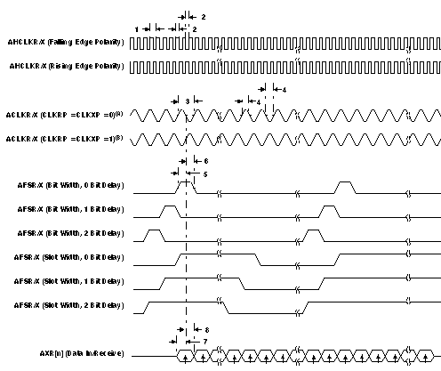
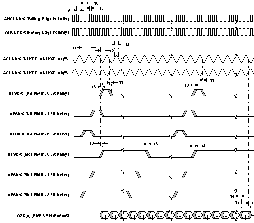
6.15 Serial Peripheral Interface Ports (SPI0, SPI1)
Figure 6-31 is a block diagram of the SPI module, which is a simple shift register and buffer plus control logic. Data is written to the shift register before transmission occurs and is read from the buffer at the end of transmission. The SPI can operate either as a master, in which case, it initiates a transfer and drives the SPIx_CLK pin, or as a slave. Four clock phase and polarity options are supported as well as many data formatting options.
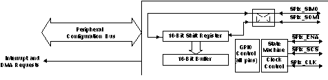 Figure 6-31 Block Diagram of SPI Module
The SPI supports 3-, 4-, and 5-pin operation with three basic pins (SPIx_CLK, SPIx_SIMO, and SPIx_SOMI) and two optional pins (SPIx_SCS, SPIx_ENA).
The optional SPIx_SCS (Slave Chip Select) pin is most useful to enable in slave mode when there are other slave devices on the same SPI port. The device will only shift data and drive the SPIx_SOMI pin when SPIx_SCS is held low.
In slave mode, SPIx_ENA is an optional output. The SPIx_ENA output provides the status of the internal transmit buffer (SPIDAT0/1 registers). In four-pin mode with the enable option, SPIx_ENA is asserted only when the transmit buffer is full, indicating that the slave is ready to begin another transfer. In five-pin mode, the SPIx_ENA is additionally qualified by SPIx_SCS being asserted. This allows a single handshake line to be shared by multiple slaves on the same SPI bus.
In master mode, the SPIx_ENA pin is an optional input and the master can be configured to delay the start of the next transfer until the slave asserts SPIx_ENA. The addition of this handshake signal simplifies SPI communications and, on average, increases SPI bus throughput since the master does not need to delay each transfer long enough to allow for the worst-case latency of the slave device. Instead, each transfer can begin as soon as both the master and slave have actually serviced the previous SPI transfer.
 Figure 6-32 Illustration of SPI Master-to-SPI Slave Connection
6.15.1 SPI Peripheral Registers Description(s)
Table 6-49 is a list of the SPI registers.
Table 6-49 SPIx Configuration Registers
| SPI0 BYTE ADDRESS |
SPI1 BYTE ADDRESS |
ACRONYM | DESCRIPTION |
|---|---|---|---|
| 0x01C4 1000 | 0x01F0 E000 | SPIGCR0 | Global Control Register 0 |
| 0x01C4 1004 | 0x01F0 E004 | SPIGCR1 | Global Control Register 1 |
| 0x01C4 1008 | 0x01F0 E008 | SPIINT0 | Interrupt Register |
| 0x01C4 100C | 0x01F0 E00C | SPILVL | Interrupt Level Register |
| 0x01C4 1010 | 0x01F0 E010 | SPIFLG | Flag Register |
| 0x01C4 1014 | 0x01F0 E014 | SPIPC0 | Pin Control Register 0 (Pin Function) |
| 0x01C4 1018 | 0x01F0 E018 | SPIPC1 | Pin Control Register 1 (Pin Direction) |
| 0x01C4 101C | 0x01F0 E01C | SPIPC2 | Pin Control Register 2 (Pin Data In) |
| 0x01C4 1020 | 0x01F0 E020 | SPIPC3 | Pin Control Register 3 (Pin Data Out) |
| 0x01C4 1024 | 0x01F0 E024 | SPIPC4 | Pin Control Register 4 (Pin Data Set) |
| 0x01C4 1028 | 0x01F0 E028 | SPIPC5 | Pin Control Register 5 (Pin Data Clear) |
| 0x01C4 102C | 0x01F0 E02C | Reserved | Reserved - Do not write to this register |
| 0x01C4 1030 | 0x01F0 E030 | Reserved | Reserved - Do not write to this register |
| 0x01C4 1034 | 0x01F0 E034 | Reserved | Reserved - Do not write to this register |
| 0x01C4 1038 | 0x01F0 E038 | SPIDAT0 | Shift Register 0 (without format select) |
| 0x01C4 103C | 0x01F0 E03C | SPIDAT1 | Shift Register 1 (with format select) |
| 0x01C4 1040 | 0x01F0 E040 | SPIBUF | Buffer Register |
| 0x01C4 1044 | 0x01F0 E044 | SPIEMU | Emulation Register |
| 0x01C4 1048 | 0x01F0 E048 | SPIDELAY | Delay Register |
| 0x01C4 104C | 0x01F0 E04C | SPIDEF | Default Chip Select Register |
| 0x01C4 1050 | 0x01F0 E050 | SPIFMT0 | Format Register 0 |
| 0x01C4 1054 | 0x01F0 E054 | SPIFMT1 | Format Register 1 |
| 0x01C4 1058 | 0x01F0 E058 | SPIFMT2 | Format Register 2 |
| 0x01C4 105C | 0x01F0 E05C | SPIFMT3 | Format Register 3 |
| 0x01C4 1060 | 0x01F0 E060 | INTVEC0 | Interrupt Vector for SPI INT0 |
| 0x01C4 1064 | 0x01F0 E064 | INTVEC1 | Interrupt Vector for SPI INT1 |
6.15.2 SPI Electrical Data/Timing
6.15.2.1 Serial Peripheral Interface (SPI) Timing
Table 6-50 through Table 6-65 assume testing over recommended operating conditions (see Figure 6-33 through Figure 6-36).
Table 6-50 General Timing Requirements for SPI0 Master Modes(1)
| NO. | 1.2V | 1.1V | 1.0V | UNIT | ||||||
|---|---|---|---|---|---|---|---|---|---|---|
| MIN | MAX | MIN | MAX | MIN | MAX | |||||
| 1 | tc(SPC)M | Cycle Time, SPI0_CLK, All Master Modes | 20(2) | 256P | 30(2) | 256P | 40(2) | 256P | ns | |
| 2 | tw(SPCH)M | Pulse Width High, SPI0_CLK, All Master Modes | 0.5M-1 | 0.5M-1 | 0.5M-1 | ns | ||||
| 3 | tw(SPCL)M | Pulse Width Low, SPI0_CLK, All Master Modes | 0.5M-1 | 0.5M-1 | 0.5M-1 | ns | ||||
| 4 | td(SIMO_SPC)M | Delay, initial data bit valid on SPI0_SIMO after initial edge on SPI0_CLK(3) | Polarity = 0, Phase = 0, to SPI0_CLK rising |
5 | 5 | 6 | ns | |||
| Polarity = 0, Phase = 1, to SPI0_CLK rising |
-0.5M+5 | -0.5M+5 | -0.5M+6 | |||||||
| Polarity = 1, Phase = 0, to SPI0_CLK falling |
5 | 5 | 6 | |||||||
| Polarity = 1, Phase = 1, to SPI0_CLK falling |
-0.5M+5 | -0.5M+5 | -0.5M+6 | |||||||
| 5 | td(SPC_SIMO)M | Delay, subsequent bits valid on SPI0_SIMO after transmit edge of SPI0_CLK | Polarity = 0, Phase = 0, from SPI0_CLK rising |
5 | 5 | 6 | ns | |||
| Polarity = 0, Phase = 1, from SPI0_CLK falling |
5 | 5 | 6 | |||||||
| Polarity = 1, Phase = 0, from SPI0_CLK falling |
5 | 5 | 6 | |||||||
| Polarity = 1, Phase = 1, from SPI0_CLK rising |
5 | 5 | 6 | |||||||
| 6 | toh(SPC_SIMO)M | Output hold time, SPI0_SIMO valid after receive edge of SPI0_CLK | Polarity = 0, Phase = 0, from SPI0_CLK falling |
0.5M-3 | 0.5M-3 | 0.5M-3 | ns | |||
| Polarity = 0, Phase = 1, from SPI0_CLK rising |
0.5M-3 | 0.5M-3 | 0.5M-3 | |||||||
| Polarity = 1, Phase = 0, from SPI0_CLK rising |
0.5M-3 | 0.5M-3 | 0.5M-3 | |||||||
| Polarity = 1, Phase = 1, from SPI0_CLK falling |
0.5M-3 | 0.5M-3 | 0.5M-3 | |||||||
| 7 | tsu(SOMI_SPC)M | Input Setup Time, SPI0_SOMI valid before receive edge of SPI0_CLK | Polarity = 0, Phase = 0, to SPI0_CLK falling |
1.5 | 1.5 | 1.5 | ns | |||
| Polarity = 0, Phase = 1, to SPI0_CLK rising |
1.5 | 1.5 | 1.5 | |||||||
| Polarity = 1, Phase = 0, to SPI0_CLK rising |
1.5 | 1.5 | 1.5 | |||||||
| Polarity = 1, Phase = 1, to SPI0_CLK falling |
1.5 | 1.5 | 1.5 | |||||||
| 8 | tih(SPC_SOMI)M | Input Hold Time, SPI0_SOMI valid after receive edge of SPI0_CLK | Polarity = 0, Phase = 0, from SPI0_CLK falling |
4 | 4 | 5 | ns | |||
| Polarity = 0, Phase = 1, from SPI0_CLK rising |
4 | 4 | 5 | |||||||
| Polarity = 1, Phase = 0, from SPI0_CLK rising |
4 | 4 | 5 | |||||||
| Polarity = 1, Phase = 1, from SPI0_CLK falling |
4 | 4 | 5 | |||||||
Table 6-51 General Timing Requirements for SPI0 Slave Modes(1)
| NO. | 1.2V | 1.1V | 1.0V | UNIT | ||||||
|---|---|---|---|---|---|---|---|---|---|---|
| MIN | MAX | MIN | MAX | MIN | MAX | |||||
| 9 | tc(SPC)S | Cycle Time, SPI0_CLK, All Slave Modes | 40(2) | 50(2) | 60(2) | ns | ||||
| 10 | tw(SPCH)S | Pulse Width High, SPI0_CLK, All Slave Modes | 18 | 22 | 27 | ns | ||||
| 11 | tw(SPCL)S | Pulse Width Low, SPI0_CLK, All Slave Modes | 18 | 22 | 27 | ns | ||||
| 12 | tsu(SOMI_SPC)S | Setup time, transmit data written to SPI before initial clock edge from master.(3)(4) |
Polarity = 0, Phase = 0, to SPI0_CLK rising |
2P | 2P | 2P | ns | |||
| Polarity = 0, Phase = 1, to SPI0_CLK rising |
2P | 2P | 2P | |||||||
| Polarity = 1, Phase = 0, to SPI0_CLK falling |
2P | 2P | 2P | |||||||
| Polarity = 1, Phase = 1, to SPI0_CLK falling |
2P | 2P | 2P | |||||||
| 13 | td(SPC_SOMI)S | Delay, subsequent bits valid on SPI0_SOMI after transmit edge of SPI0_CLK | Polarity = 0, Phase = 0, from SPI0_CLK rising |
17 | 20 | 27 | ns | |||
| Polarity = 0, Phase = 1, from SPI0_CLK falling |
17 | 20 | 27 | |||||||
| Polarity = 1, Phase = 0, from SPI0_CLK falling |
17 | 20 | 27 | |||||||
| Polarity = 1, Phase = 1, from SPI0_CLK rising |
17 | 20 | 27 | |||||||
| 14 | toh(SPC_SOMI)S | Output hold time, SPI0_SOMI valid after receive edge of SPI0_CLK | Polarity = 0, Phase = 0, from SPI0_CLK falling |
0.5S-6 | 0.5S-16 | 0.5S-20 | ns | |||
| Polarity = 0, Phase = 1, from SPI0_CLK rising |
0.5S-6 | 0.5S-16 | 0.5S-20 | |||||||
| Polarity = 1, Phase = 0, from SPI0_CLK rising |
0.5S-6 | 0.5S-16 | 0.5S-20 | |||||||
| Polarity = 1, Phase = 1, from SPI0_CLK falling |
0.5S-6 | 0.5S-16 | 0.5S-20 | |||||||
| 15 | tsu(SIMO_SPC)S | Input Setup Time, SPI0_SIMO valid before receive edge of SPI0_CLK | Polarity = 0, Phase = 0, to SPI0_CLK falling |
1.5 | 1.5 | 1.5 | ns | |||
| Polarity = 0, Phase = 1, to SPI0_CLK rising |
1.5 | 1.5 | 1.5 | |||||||
| Polarity = 1, Phase = 0, to SPI0_CLK rising |
1.5 | 1.5 | 1.5 | |||||||
| Polarity = 1, Phase = 1, to SPI0_CLK falling |
1.5 | 1.5 | 1.5 | |||||||
| 16 | tih(SPC_SIMO)S | Input Hold Time, SPI0_SIMO valid after receive edge of SPI0_CLK | Polarity = 0, Phase = 0, from SPI0_CLK falling |
4 | 4 | 5 | ns | |||
| Polarity = 0, Phase = 1, from SPI0_CLK rising |
4 | 4 | 5 | |||||||
| Polarity = 1, Phase = 0, from SPI0_CLK rising |
4 | 4 | 5 | |||||||
| Polarity = 1, Phase = 1, from SPI0_CLK falling |
4 | 4 | 5 | |||||||
Table 6-52 Additional SPI0 Master Timings, 4-Pin Enable Option (5)(1)(2)
| NO. | PARAMETER | 1.2V | 1.1V | 1.0V | UNIT | |||||
|---|---|---|---|---|---|---|---|---|---|---|
| MIN | MAX | MIN | MAX | MIN | MAX | |||||
| 17 | td(ENA_SPC)M | Delay from slave assertion of SPI0_ENA active to first SPI0_CLK from master.(3) | Polarity = 0, Phase = 0, to SPI0_CLK rising |
3P+5 | 3P+5 | 3P+6 | ns | |||
| Polarity = 0, Phase = 1, to SPI0_CLK rising |
0.5M+3P+5 | 0.5M+3P+5 | 0.5M+3P+6 | |||||||
| Polarity = 1, Phase = 0, to SPI0_CLK falling |
3P+5 | 3P+5 | 3P+6 | |||||||
| Polarity = 1, Phase = 1, to SPI0_CLK falling |
0.5M+3P+5 | 0.5M+3P+5 | 0.5M+3P+6 | |||||||
| 18 | td(SPC_ENA)M | Max delay for slave to deassert SPI0_ENA after final SPI0_CLK edge to ensure master does not begin the next transfer.(4) | Polarity = 0, Phase = 0, from SPI0_CLK falling |
0.5M+P+5 | 0.5M+P+5 | 0.5M+P+6 | ns | |||
| Polarity = 0, Phase = 1, from SPI0_CLK falling |
P+5 | P+5 | P+6 | |||||||
| Polarity = 1, Phase = 0, from SPI0_CLK rising |
0.5M+P+5 | 0.5M+P+5 | 0.5M+P+6 | |||||||
| Polarity = 1, Phase = 1, from SPI0_CLK rising |
P+5 | P+5 | P+6 | |||||||
Table 6-53 Additional SPI0 Master Timings, 4-Pin Chip Select Option (7)(1)(2)
| NO. | PARAMETER | 1.2V | 1.1V | 1.0V | UNIT | |||||
|---|---|---|---|---|---|---|---|---|---|---|
| MIN | MAX | MIN | MAX | MIN | MAX | |||||
| 19 | td(SCS_SPC)M | Delay from SPI0_SCS active to first SPI0_CLK(3)(4) | Polarity = 0, Phase = 0, to SPI0_CLK rising |
2P-1 | 2P-2 | 2P-3 | ns | |||
| Polarity = 0, Phase = 1, to SPI0_CLK rising |
0.5M+2P-1 | 0.5M+2P-2 | 0.5M+2P-3 | |||||||
| Polarity = 1, Phase = 0, to SPI0_CLK falling |
2P-1 | 2P-2 | 2P-3 | |||||||
| Polarity = 1, Phase = 1, to SPI0_CLK falling |
0.5M+2P-1 | 0.5M+2P-2 | 0.5M+2P-3 | |||||||
| 20 | td(SPC_SCS)M | Delay from final SPI0_CLK edge to master deasserting SPI0_SCS(5)(6) | Polarity = 0, Phase = 0, from SPI0_CLK falling |
0.5M+P-1 | 0.5M+P-2 | 0.5M+P-3 | ns | |||
| Polarity = 0, Phase = 1, from SPI0_CLK falling |
P-1 | P-2 | P-3 | |||||||
| Polarity = 1, Phase = 0, from SPI0_CLK rising |
0.5M+P-1 | 0.5M+P-2 | 0.5M+P-3 | |||||||
| Polarity = 1, Phase = 1, from SPI0_CLK rising |
P-1 | P-2 | P-3 | |||||||
Table 6-54 Additional SPI0 Master Timings, 5-Pin Option (10)(1)(2)
| NO. | PARAMETER | 1.2V | 1.1V | 1.0V | UNIT | |||||
|---|---|---|---|---|---|---|---|---|---|---|
| MIN | MAX | MIN | MAX | MIN | MAX | |||||
| 18 | td(SPC_ENA)M | Max delay for slave to deassert SPI0_ENA after final SPI0_CLK edge to ensure master does not begin the next transfer.(3) | Polarity = 0, Phase = 0, from SPI0_CLK falling |
0.5M+P+5 | 0.5M+P+5 | 0.5M+P+6 | ns | |||
| Polarity = 0, Phase = 1, from SPI0_CLK falling |
P+5 | P+5 | P+6 | |||||||
| Polarity = 1, Phase = 0, from SPI0_CLK rising |
0.5M+P+5 | 0.5M+P+5 | 0.5M+P+6 | |||||||
| Polarity = 1, Phase = 1, from SPI0_CLK rising |
P+5 | P+5 | P+6 | |||||||
| 20 | td(SPC_SCS)M | Delay from final SPI0_CLK edge to master deasserting SPI0_SCS(4)(5) |
Polarity = 0, Phase = 0, from SPI0_CLK falling |
0.5M+P-2 | 0.5M+P-2 | 0.5M+P-3 | ns | |||
| Polarity = 0, Phase = 1, from SPI0_CLK falling |
P-2 | P-2 | P-3 | |||||||
| Polarity = 1, Phase = 0, from SPI0_CLK rising |
0.5M+P-2 | 0.5M+P-2 | 0.5M+P-3 | |||||||
| Polarity = 1, Phase = 1, from SPI0_CLK rising |
P-2 | P-2 | P-3 | |||||||
| 21 | td(SCSL_ENAL)M | Max delay for slave SPI to drive SPI0_ENA valid after master asserts SPI0_SCS to delay the master from beginning the next transfer, | C2TDELAY+P | C2TDELAY+P | C2TDELAY+P | ns | ||||
| 22 | td(SCS_SPC)M | Delay from SPI0_SCS active to first SPI0_CLK(6)(7)(8) | Polarity = 0, Phase = 0, to SPI0_CLK rising |
2P-2 | 2P-2 | 2P-3 | ns | |||
| Polarity = 0, Phase = 1, to SPI0_CLK rising |
0.5M+2P-2 | 0.5M+2P-2 | 0.5M+2P-3 | |||||||
| Polarity = 1, Phase = 0, to SPI0_CLK falling |
2P-2 | 2P-2 | 2P-3 | |||||||
| Polarity = 1, Phase = 1, to SPI0_CLK falling |
0.5M+2P-2 | 0.5M+2P-2 | 0.5M+2P-3 | |||||||
| 23 | td(ENA_SPC)M | Delay from assertion of SPI0_ENA low to first SPI0_CLK edge.(9) | Polarity = 0, Phase = 0, to SPI0_CLK rising |
3P+5 | 3P+5 | 3P+6 | ns | |||
| Polarity = 0, Phase = 1, to SPI0_CLK rising |
0.5M+3P+5 | 0.5M+3P+5 | 0.5M+3P+6 | |||||||
| Polarity = 1, Phase = 0, to SPI0_CLK falling |
3P+5 | 3P+5 | 3P+6 | |||||||
| Polarity = 1, Phase = 1, to SPI0_CLK falling |
0.5M+3P+5 | 0.5M+3P+5 | 0.5M+3P+6 | |||||||
Table 6-55 Additional SPI0 Slave Timings, 4-Pin Enable Option (3)(1)(2)
| NO. | PARAMETER | 1.2V | 1.1V | 1.0V | UNIT | |||||
|---|---|---|---|---|---|---|---|---|---|---|
| MIN | MAX | MIN | MAX | MIN | MAX | |||||
| 24 | td(SPC_ENAH)S | Delay from final SPI0_CLK edge to slave deasserting SPI0_ENA. | Polarity = 0, Phase = 0, from SPI0_CLK falling |
1.5P-3 | 2.5P+17.5 | 1.5P-3 | 2.5P+20 | 1.5P-3 | 2.5P+27 | ns |
| Polarity = 0, Phase = 1, from SPI0_CLK falling |
- 0.5M+1.5P-3 | - 0.5M+2.5P+17.5 | - 0.5M+1.5P-3 | - 0.5M+2.5P+20 | - 0.5M+1.5P-3 | - 0.5M+2.5P+27 | ||||
| Polarity = 1, Phase = 0, from SPI0_CLK rising |
1.5P-3 | 2.5P+17.5 | 1.5P-3 | 2.5P+20 | 1.5P-3 | 2.5P+27 | ||||
| Polarity = 1, Phase = 1, from SPI0_CLK rising |
- 0.5M+1.5P-3 | - 0.5+2.5P+17.5 | - 0.5M+1.5P-3 | - 0.5+2.5P+20 | - 0.5M+1.5P-3 | - 0.5+2.5P+27 | ||||
Table 6-56 Additional SPI0 Slave Timings, 4-Pin Chip Select Option (3)(1)(2)
| NO. | PARAMETER | 1.2V | 1.1V | 1.0V | UNIT | |||||
|---|---|---|---|---|---|---|---|---|---|---|
| MIN | MAX | MIN | MAX | MIN | MAX | |||||
| 25 | td(SCSL_SPC)S | Required delay from SPI0_SCS asserted at slave to first SPI0_CLK edge at slave. | P + 1.5 | P + 1.5 | P + 1.5 | ns | ||||
| 26 | td(SPC_SCSH)S | Required delay from final SPI0_CLK edge before SPI0_SCS is deasserted. | Polarity = 0, Phase = 0, from SPI0_CLK falling |
0.5M+P+4 | 0.5M+P+4 | 0.5M+P+5 | ns | |||
| Polarity = 0, Phase = 1, from SPI0_CLK falling |
P+4 | P+4 | P+5 | |||||||
| Polarity = 1, Phase = 0, from SPI0_CLK rising |
0.5M+P+4 | 0.5M+P+4 | 0.5M+P+5 | |||||||
| Polarity = 1, Phase = 1, from SPI0_CLK rising |
P+4 | P+4 | P+5 | |||||||
| 27 | tena(SCSL_SOMI)S | Delay from master asserting SPI0_SCS to slave driving SPI0_SOMI valid | P+17.5 | P+20 | P+27 | ns | ||||
| 28 | tdis(SCSH_SOMI)S | Delay from master deasserting SPI0_SCS to slave 3-stating SPI0_SOMI | P+17.5 | P+20 | P+27 | ns | ||||
Table 6-57 Additional SPI0 Slave Timings, 5-Pin Option (4)(1)(2)
| NO. | PARAMETER | 1.2V | 1.1V | 1.0V | UNIT | |||||
|---|---|---|---|---|---|---|---|---|---|---|
| MIN | MAX | MIN | MAX | MIN | MAX | |||||
| 25 | td(SCSL_SPC)S | Required delay from SPI0_SCS asserted at slave to first SPI0_CLK edge at slave. | P + 1.5 | P + 1.5 | P + 1.5 | ns | ||||
| 26 | td(SPC_SCSH)S | Required delay from final SPI0_CLK edge before SPI0_SCS is deasserted. | Polarity = 0, Phase = 0, from SPI0_CLK falling |
0.5M+P+4 | 0.5M+P+4 | 0.5M+P+5 | ns | |||
| Polarity = 0, Phase = 1, from SPI0_CLK falling |
P+4 | P+4 | P+5 | |||||||
| Polarity = 1, Phase = 0, from SPI0_CLK rising |
0.5M+P+4 | 0.5M+P+4 | 0.5M+P+5 | |||||||
| Polarity = 1, Phase = 1, from SPI0_CLK rising |
P+4 | P+4 | P+5 | |||||||
| 27 | tena(SCSL_SOMI)S | Delay from master asserting SPI0_SCS to slave driving SPI0_SOMI valid | P+17.5 | P+20 | P+27 | ns | ||||
| 28 | tdis(SCSH_SOMI)S | Delay from master deasserting SPI0_SCS to slave 3-stating SPI0_SOMI | P+17.5 | P+20 | P+27 | ns | ||||
| 29 | tena(SCSL_ENA)S | Delay from master deasserting SPI0_SCS to slave driving SPI0_ENA valid | 17.5 | 20 | 27 | ns | ||||
| 30 | tdis(SPC_ENA)S | Delay from final clock receive edge on SPI0_CLK to slave 3-stating or driving high SPI0_ENA.(3) | Polarity = 0, Phase = 0, from SPI0_CLK falling |
2.5P+17.5 | 2.5P+20 | 2.5P+27 | ns | |||
| Polarity = 0, Phase = 1, from SPI0_CLK rising |
2.5P+17.5 | 2.5P+20 | 2.5P+27 | |||||||
| Polarity = 1, Phase = 0, from SPI0_CLK rising |
2.5P+17.5 | 2.5P+20 | 2.5P+27 | |||||||
| Polarity = 1, Phase = 1, from SPI0_CLK falling |
2.5P+17.5 | 2.5P+20 | 2.5P+27 | |||||||
Table 6-58 General Timing Requirements for SPI1 Master Modes(1)
| NO. | 1.2V | 1.1V | 1.0V | UNIT | ||||||
|---|---|---|---|---|---|---|---|---|---|---|
| MIN | MAX | MIN | MAX | MIN | MAX | |||||
| 1 | tc(SPC)M | Cycle Time, SPI1_CLK, All Master Modes | 20(2) | 256P | 30(2) | 256P | 40(2) | 256P | ns | |
| 2 | tw(SPCH)M | Pulse Width High, SPI1_CLK, All Master Modes | 0.5M-1 | 0.5M-1 | 0.5M-1 | ns | ||||
| 3 | tw(SPCL)M | Pulse Width Low, SPI1_CLK, All Master Modes | 0.5M-1 | 0.5M-1 | 0.5M-1 | ns | ||||
| 4 | td(SIMO_SPC)M | Delay, initial data bit valid on SPI1_SIMO to initial edge on SPI1_CLK(3) | Polarity = 0, Phase = 0, to SPI1_CLK rising |
5 | 5 | 6 | ns | |||
| Polarity = 0, Phase = 1, to SPI1_CLK rising |
-0.5M+5 | -0.5M+5 | -0.5M+6 | |||||||
| Polarity = 1, Phase = 0, to SPI1_CLK falling |
5 | 5 | 6 | |||||||
| Polarity = 1, Phase = 1, to SPI1_CLK falling |
-0.5M+5 | -0.5M+5 | -0.5M+6 | |||||||
| 5 | td(SPC_SIMO)M | Delay, subsequent bits valid on SPI1_SIMO after transmit edge of SPI1_CLK | Polarity = 0, Phase = 0, from SPI1_CLK rising |
5 | 5 | 6 | ns | |||
| Polarity = 0, Phase = 1, from SPI1_CLK falling |
5 | 5 | 6 | |||||||
| Polarity = 1, Phase = 0, from SPI1_CLK falling |
5 | 5 | 6 | |||||||
| Polarity = 1, Phase = 1, from SPI1_CLK rising |
5 | 5 | 6 | |||||||
| 6 | toh(SPC_SIMO)M | Output hold time, SPI1_SIMO valid after receive edge of SPI1_CLK | Polarity = 0, Phase = 0, from SPI1_CLK falling |
0.5M-3 | 0.5M-3 | 0.5M-3 | ns | |||
| Polarity = 0, Phase = 1, from SPI1_CLK rising |
0.5M-3 | 0.5M-3 | 0.5M-3 | |||||||
| Polarity = 1, Phase = 0, from SPI1_CLK rising |
0.5M-3 | 0.5M-3 | 0.5M-3 | |||||||
| Polarity = 1, Phase = 1, from SPI1_CLK falling |
0.5M-3 | 0.5M-3 | 0.5M-3 | |||||||
| 7 | tsu(SOMI_SPC)M | Input Setup Time, SPI1_SOMI valid before receive edge of SPI1_CLK | Polarity = 0, Phase = 0, to SPI1_CLK falling |
1.5 | 1.5 | 1.5 | ns | |||
| Polarity = 0, Phase = 1, to SPI1_CLK rising |
1.5 | 1.5 | 1.5 | |||||||
| Polarity = 1, Phase = 0, to SPI1_CLK rising |
1.5 | 1.5 | 1.5 | |||||||
| Polarity = 1, Phase = 1, to SPI1_CLK falling |
1.5 | 1.5 | 1.5 | |||||||
| 8 | tih(SPC_SOMI)M | Input Hold Time, SPI1_SOMI valid after receive edge of SPI1_CLK | Polarity = 0, Phase = 0, from SPI1_CLK falling |
4 | 5 | 6 | ns | |||
| Polarity = 0, Phase = 1, from SPI1_CLK rising |
4 | 5 | 6 | |||||||
| Polarity = 1, Phase = 0, from SPI1_CLK rising |
4 | 5 | 6 | |||||||
| Polarity = 1, Phase = 1, from SPI1_CLK falling |
4 | 5 | 6 | |||||||
Table 6-59 General Timing Requirements for SPI1 Slave Modes(1)
| NO. | 1.2V | 1.1V | 1.0V | UNIT | ||||||
|---|---|---|---|---|---|---|---|---|---|---|
| MIN | MAX | MIN | MAX | MIN | MAX | |||||
| 9 | tc(SPC)S | Cycle Time, SPI1_CLK, All Slave Modes | 40(2) | 50(2) | 60(2) | ns | ||||
| 10 | tw(SPCH)S | Pulse Width High, SPI1_CLK, All Slave Modes | 18 | 22 | 27 | ns | ||||
| 11 | tw(SPCL)S | Pulse Width Low, SPI1_CLK, All Slave Modes | 18 | 22 | 27 | ns | ||||
| 12 | tsu(SOMI_SPC)S | Setup time, transmit data written to SPI before initial clock edge from master.(3)(4) |
Polarity = 0, Phase = 0, to SPI1_CLK rising |
2P | 2P | 2P | ns | |||
| Polarity = 0, Phase = 1, to SPI1_CLK rising |
2P | 2P | 2P | |||||||
| Polarity = 1, Phase = 0, to SPI1_CLK falling |
2P | 2P | 2P | |||||||
| Polarity = 1, Phase = 1, to SPI1_CLK falling |
2P | 2P | 2P | |||||||
| 13 | td(SPC_SOMI)S | Delay, subsequent bits valid on SPI1_SOMI after transmit edge of SPI1_CLK | Polarity = 0, Phase = 0, from SPI1_CLK rising |
15 | 17 | 19 | ns | |||
| Polarity = 0, Phase = 1, from SPI1_CLK falling |
15 | 17 | 19 | |||||||
| Polarity = 1, Phase = 0, from SPI1_CLK falling |
15 | 17 | 19 | |||||||
| Polarity = 1, Phase = 1, from SPI1_CLK rising |
15 | 17 | 19 | |||||||
| 14 | toh(SPC_SOMI)S | Output hold time, SPI1_SOMI valid after receive edge of SPI1_CLK | Polarity = 0, Phase = 0, from SPI1_CLK falling |
0.5S-4 | 0.5S-10 | 0.5S-12 | ns | |||
| Polarity = 0, Phase = 1, from SPI1_CLK rising |
0.5S-4 | 0.5S-10 | 0.5S-12 | |||||||
| Polarity = 1, Phase = 0, from SPI1_CLK rising |
0.5S-4 | 0.5S-10 | 0.5S-12 | |||||||
| Polarity = 1, Phase = 1, from SPI1_CLK falling |
0.5S-4 | 0.5S-10 | 0.5S-12 | |||||||
| 15 | tsu(SIMO_SPC)S | Input Setup Time, SPI1_SIMO valid before receive edge of SPI1_CLK | Polarity = 0, Phase = 0, to SPI1_CLK falling |
1.5 | 1.5 | 1.5 | ns | |||
| Polarity = 0, Phase = 1, to SPI1_CLK rising |
1.5 | 1.5 | 1.5 | |||||||
| Polarity = 1, Phase = 0, to SPI1_CLK rising |
1.5 | 1.5 | 1.5 | |||||||
| Polarity = 1, Phase = 1, to SPI1_CLK falling |
1.5 | 1.5 | 1.5 | |||||||
| 16 | tih(SPC_SIMO)S | Input Hold Time, SPI1_SIMO valid after receive edge of SPI1_CLK | Polarity = 0, Phase = 0, from SPI1_CLK falling |
4 | 5 | 6 | ns | |||
| Polarity = 0, Phase = 1, from SPI1_CLK rising |
4 | 5 | 6 | |||||||
| Polarity = 1, Phase = 0, from SPI1_CLK rising |
4 | 5 | 6 | |||||||
| Polarity = 1, Phase = 1, from SPI1_CLK falling |
4 | 5 | 6 | |||||||
Table 6-60 Additional(5) SPI1 Master Timings, 4-Pin Enable Option(1)(2)
| NO. | PARAMETER | 1.2V | 1.1V | 1.0V | UNIT | |||||
|---|---|---|---|---|---|---|---|---|---|---|
| MIN | MAX | MIN | MAX | MIN | MAX | |||||
| 17 | td(EN A_SPC)M | Delay from slave assertion of SPI1_ENA active to first SPI1_CLK from master.(3) | Polarity = 0, Phase = 0, to SPI1_CLK rising |
3P+5 | 3P+5 | 3P+6 | ns | |||
| Polarity = 0, Phase = 1, to SPI1_CLK rising |
0.5M+3P+5 | 0.5M+3P+5 | 0.5M+3P+6 | |||||||
| Polarity = 1, Phase = 0, to SPI1_CLK falling |
3P+5 | 3P+5 | 3P+6 | |||||||
| Polarity = 1, Phase = 1, to SPI1_CLK falling |
0.5M+3P+5 | 0.5M+3P+5 | 0.5M+3P+6 | |||||||
| 18 | td(SPC_ENA)M | Max delay for slave to deassert SPI1_ENA after final SPI1_CLK edge to ensure master does not begin the next transfer.(4) | Polarity = 0, Phase = 0, from SPI1_CLK falling |
0.5M+P+5 | 0.5M+P+5 | 0.5M+P+6 | ns | |||
| Polarity = 0, Phase = 1, from SPI1_CLK falling |
P+5 | P+5 | P+6 | |||||||
| Polarity = 1, Phase = 0, from SPI1_CLK rising |
0.5M+P+5 | 0.5M+P+5 | 0.5M+P+6 | |||||||
| Polarity = 1, Phase = 1, from SPI1_CLK rising |
P+5 | P+5 | P+6 | |||||||
Table 6-61 Additional(7) SPI1 Master Timings, 4-Pin Chip Select Option(1)(2)
| NO. | PARAMETER | 1.2V | 1.1V | 1.0V | UNIT | |||||
|---|---|---|---|---|---|---|---|---|---|---|
| MIN | MAX | MIN | MAX | MIN | MAX | |||||
| 19 | td(SCS_SPC)M | Delay from SPI1_SCS active to first SPI1_CLK(3)(4) | Polarity = 0, Phase = 0, to SPI1_CLK rising |
2P-1 | 2P-5 | 2P-6 | ns | |||
| Polarity = 0, Phase = 1, to SPI1_CLK rising |
0.5M+2P-1 | 0.5M+2P-5 | 0.5M+2P-6 | |||||||
| Polarity = 1, Phase = 0, to SPI1_CLK falling |
2P-1 | 2P-5 | 2P-6 | |||||||
| Polarity = 1, Phase = 1, to SPI1_CLK falling |
0.5M+2P-1 | 0.5M+2P-5 | 0.5M+2P-6 | |||||||
| 20 | td(SPC_SCS)M | Delay from final SPI1_CLK edge to master deasserting SPI1_SCS(5)(6) | Polarity = 0, Phase = 0, from SPI1_CLK falling |
0.5M+P-1 | 0.5M+P-5 | 0.5M+P-6 | ns | |||
| Polarity = 0, Phase = 1, from SPI1_CLK falling |
P-1 | P-5 | P-6 | |||||||
| Polarity = 1, Phase = 0, from SPI1_CLK rising |
0.5M+P-1 | 0.5M+P-5 | 0.5M+P-6 | |||||||
| Polarity = 1, Phase = 1, from SPI1_CLK rising |
P-1 | P-5 | P-6 | |||||||
Table 6-62 Additional(10) SPI1 Master Timings, 5-Pin Option(1)(2)
| NO. | PARAMETER | 1.3V, 1.2V | 1.1V | 1.0V | UNIT | |||||
|---|---|---|---|---|---|---|---|---|---|---|
| MIN | MAX | MIN | MAX | MIN | MAX | |||||
| 18 | td(SPC_ENA)M | Max delay for slave to deassert SPI1_ENA after final SPI1_CLK edge to ensure master does not begin the next transfer.(3) | Polarity = 0, Phase = 0, from SPI1_CLK falling |
0.5M+P+5 | 0.5M+P+5 | 0.5M+P+6 | ns | |||
| Polarity = 0, Phase = 1, from SPI1_CLK falling |
P+5 | P+5 | P+6 | |||||||
| Polarity = 1, Phase = 0, from SPI1_CLK rising |
0.5M+P+5 | 0.5M+P+5 | 0.5M+P+6 | |||||||
| Polarity = 1, Phase = 1, from SPI1_CLK rising |
P+5 | P+5 | P+6 | |||||||
| 20 | td(SPC_SCS)M | Delay from final SPI1_CLK edge to master deasserting SPI1_SCS(4)(5) |
Polarity = 0, Phase = 0, from SPI1_CLK falling |
0.5M+P-1 | 0.5M+P-5 | 0.5M+P-6 | ns | |||
| Polarity = 0, Phase = 1, from SPI1_CLK falling |
P-1 | P-5 | P-6 | |||||||
| Polarity = 1, Phase = 0, from SPI1_CLK rising |
0.5M+P-1 | 0.5M+P-5 | 0.5M+P-6 | |||||||
| Polarity = 1, Phase = 1, from SPI1_CLK rising |
P-1 | P-5 | P-6 | |||||||
| 21 | td(SCSL_ENAL)M | Max delay for slave SPI to drive SPI1_ENA valid after master asserts SPI1_SCS to delay the master from beginning the next transfer, |
C2TDELAY+P | C2TDELAY+P | C2TDELAY+P | ns | ||||
| 22 | td(SCS_SPC)M | Delay from SPI1_SCS active to first SPI1_CLK(6)(7)(8) | Polarity = 0, Phase = 0, to SPI1_CLK rising |
2P-1 | 2P-5 | 2P-6 | ns | |||
| Polarity = 0, Phase = 1, to SPI1_CLK rising |
0.5M+2P-1 | 0.5M+2P-5 | 0.5M+2P-6 | |||||||
| Polarity = 1, Phase = 0, to SPI1_CLK falling |
2P-1 | 2P-5 | 2P-6 | |||||||
| Polarity = 1, Phase = 1, to SPI1_CLK falling |
0.5M+2P-1 | 0.5M+2P-5 | 0.5M+2P-6 | |||||||
| 23 | td(ENA_SPC)M | Delay from assertion of SPI1_ENA low to first SPI1_CLK edge.(9) | Polarity = 0, Phase = 0, to SPI1_CLK rising |
3P+5 | 3P+5 | 3P+6 | ns | |||
| Polarity = 0, Phase = 1, to SPI1_CLK rising |
0.5M+3P+5 | 0.5M+3P+5 | 0.5M+3P+6 | |||||||
| Polarity = 1, Phase = 0, to SPI1_CLK falling |
3P+5 | 3P+5 | 3P+6 | |||||||
| Polarity = 1, Phase = 1, to SPI1_CLK falling |
0.5M+3P+5 | 0.5M+3P+5 | 0.5M+3P+6 | |||||||
Table 6-63 Additional(3) SPI1 Slave Timings, 4-Pin Enable Option(1)(2)
| NO. | PARAMETER | 1.2V | 1.1V | 1.0V | UNIT | |||||
|---|---|---|---|---|---|---|---|---|---|---|
| MIN | MAX | MIN | MAX | MIN | MAX | |||||
| 24 | td(SPC_ENAH)S | Delay from final SPI1_CLK edge to slave deasserting SPI1_ENA. | Polarity = 0, Phase = 0, from SPI1_CLK falling |
1.5P-3 | 2.5P+15 | 1.5P-10 | 2.5P+17 | 1.5P-12 | 2.5P+19 | ns |
| Polarity = 0, Phase = 1, from SPI1_CLK falling |
-0.5M+1.5P-3 | -0.5M+2.5P+15 | -0.5M+1.5P-10 | -0.5M+2.5P+17 | -0.5M+1.5P-12 | -0.5M+2.5P+19 | ||||
| Polarity = 1, Phase = 0, from SPI1_CLK rising |
1.5P-3 | 2.5P+15 | 1.5P-10 | 2.5P+17 | 1.5P-12 | 2.5P+19 | ||||
| Polarity = 1, Phase = 1, from SPI1_CLK rising |
-0.5M+1.5P-3 | -0.5M+2.5P+15 | -0.5M+1.5P-10 | -0.5M+2.5P+17 | -0.5M+1.5P-12 | -0.5M+2.5P+19 | ||||
Table 6-64 Additional(3) SPI1 Slave Timings, 4-Pin Chip Select Option(1)(2)
| NO. | PARAMETER | 1.3V, 1.2V | 1.1V | 1.0V | UNIT | |||||
|---|---|---|---|---|---|---|---|---|---|---|
| MIN | MAX | MIN | MAX | MIN | MAX | |||||
| 25 | td(SCSL_SPC)S | Required delay from SPI1_SCS asserted at slave to first SPI1_CLK edge at slave. | P+1.5 | P+1.5 | P+1.5 | ns | ||||
| 26 | td(SPC_SCSH)S | Required delay from final SPI1_CLK edge before SPI1_SCS is deasserted. | Polarity = 0, Phase = 0, from SPI1_CLK falling |
0.5M+P+4 | 0.5M+P+5 | 0.5M+P+6 | ns | |||
| Polarity = 0, Phase = 1, from SPI1_CLK falling |
P+4 | P+5 | P+6 | |||||||
| Polarity = 1, Phase = 0, from SPI1_CLK rising |
0.5M+P+4 | 0.5M+P+5 | 0.5M+P+6 | |||||||
| Polarity = 1, Phase = 1, from SPI1_CLK rising |
P+4 | P+5 | P+6 | |||||||
| 27 | tena(SCSL_SOMI)S | Delay from master asserting SPI1_SCS to slave driving SPI1_SOMI valid | P+15 | P+17 | P+19 | ns | ||||
| 28 | tdis(SCSH_SOMI)S | Delay from master deasserting SPI1_SCS to slave 3-stating SPI1_SOMI | P+15 | P+17 | P+19 | ns | ||||
Table 6-65 Additional(4) SPI1 Slave Timings, 5-Pin Option(1)(2)
| NO. | PARAMETER | 1.2V | 1.1V | 1.0V | UNIT | |||||
|---|---|---|---|---|---|---|---|---|---|---|
| MIN | MAX | MIN | MAX | MIN | MAX | |||||
| 25 | td(SCSL_SPC)S | Required delay from SPI1_SCS asserted at slave to first SPI1_CLK edge at slave. | P+1.5 | P+1.5 | P+1.5 | ns | ||||
| 26 | td(SPC_SCSH)S | Required delay from final SPI1_CLK edge before SPI1_SCS is deasserted. | Polarity = 0, Phase = 0, from SPI1_CLK falling |
0.5M+P+4 | 0.5M+P+5 | 0.5M+P+6 | ns | |||
| Polarity = 0, Phase = 1, from SPI1_CLK falling |
P+4 | P+5 | P+6 | |||||||
| Polarity = 1, Phase = 0, from SPI1_CLK rising |
0.5M+P+4 | 0.5M+P+5 | 0.5M+P+6 | |||||||
| Polarity = 1, Phase = 1, from SPI1_CLK rising |
P+4 | P+5 | P+6 | |||||||
| 27 | tena(SCSL_SOMI)S | Delay from master asserting SPI1_SCS to slave driving SPI1_SOMI valid | P+15 | P+17 | P+19 | ns | ||||
| 28 | tdis(SCSH_SOMI)S | Delay from master deasserting SPI1_SCS to slave 3-stating SPI1_SOMI | P+15 | P+17 | P+19 | ns | ||||
| 29 | tena(SCSL_ENA)S | Delay from master deasserting SPI1_SCS to slave driving SPI1_ENA valid | 15 | 17 | 19 | ns | ||||
| 30 | tdis(SPC_ENA)S | Delay from final clock receive edge on SPI1_CLK to slave 3-stating or driving high SPI1_ENA.(3) | Polarity = 0, Phase = 0, from SPI1_CLK falling |
2.5P+15 | 2.5P+17 | 2.5P+19 | ns | |||
| Polarity = 0, Phase = 1, from SPI1_CLK rising |
2.5P+15 | 2.5P+17 | 2.5P+19 | |||||||
| Polarity = 1, Phase = 0, from SPI1_CLK rising |
2.5P+15 | 2.5P+17 | 2.5P+19 | |||||||
| Polarity = 1, Phase = 1, from SPI1_CLK falling |
2.5P+15 | 2.5P+17 | 2.5P+19 | |||||||
 Figure 6-33 SPI Timings—Master Mode
 Figure 6-34 SPI Timings—Slave Mode
 Figure 6-35 SPI Timings—Master Mode (4-Pin and 5-Pin)
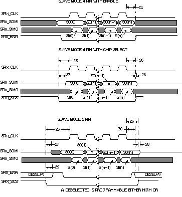 Figure 6-36 SPI Timings—Slave Mode (4-Pin and 5-Pin)
6.16 Inter-Integrated Circuit Serial Ports (I2C)
6.16.1 I2C Device-Specific Information
I2C port supports:
- Compatible with Philips® I2C Specification Revision 2.1 (January 2000)
- Fast Mode up to 400 Kbps (no fail-safe I/O buffers)
- Noise Filter to Remove Noise 50 ns or less
- Seven- and Ten-Bit Device Addressing Modes
- Master (Transmit/Receive) and Slave (Transmit/Receive) Functionality
- Events: DMA, Interrupt, or Polling
- General-Purpose I/O Capability if not used as I2C
Figure 6-37 is block diagram of the device I2C Module.
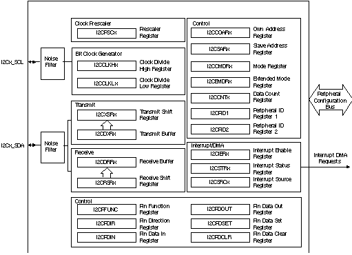 Figure 6-37 I2C Module Block Diagram
6.16.2 I2C Peripheral Registers Description(s)
Table 6-66 is the list of the I2C registers.
Table 6-66 Inter-Integrated Circuit (I2C) Registers
| I2C0 BYTE ADDRESS |
ACRONYM | REGISTER DESCRIPTION |
|---|---|---|
| 0x01C2 2000 | ICOAR | I2C Own Address Register |
| 0x01C2 2004 | ICIMR | I2C Interrupt Mask Register |
| 0x01C2 2008 | ICSTR | I2C Interrupt Status Register |
| 0x01C2 200C | ICCLKL | I2C Clock Low-Time Divider Register |
| 0x01C2 2010 | ICCLKH | I2C Clock High-Time Divider Register |
| 0x01C2 2014 | ICCNT | I2C Data Count Register |
| 0x01C2 2018 | ICDRR | I2C Data Receive Register |
| 0x01C2 201C | ICSAR | I2C Slave Address Register |
| 0x01C2 2020 | ICDXR | I2C Data Transmit Register |
| 0x01C2 2024 | ICMDR | I2C Mode Register |
| 0x01C2 2028 | ICIVR | I2C Interrupt Vector Register |
| 0x01C2 202C | ICEMDR | I2C Extended Mode Register |
| 0x01C2 2030 | ICPSC | I2C Prescaler Register |
| 0x01C2 2034 | REVID1 | I2C Revision Identification Register 1 |
| 0x01C2 2038 | REVID2 | I2C Revision Identification Register 2 |
| 0x01C2 2048 | ICPFUNC | I2C Pin Function Register |
| 0x01C2 204C | ICPDIR | I2C Pin Direction Register |
| 0x01C2 2050 | ICPDIN | I2C Pin Data In Register |
| 0x01C2 2054 | ICPDOUT | I2C Pin Data Out Register |
| 0x01C2 2058 | ICPDSET | I2C Pin Data Set Register |
| 0x01C2 205C | ICPDCLR | I2C Pin Data Clear Register |
6.16.3 I2C Electrical Data/Timing
6.16.3.1 Inter-Integrated Circuit (I2C) Timing
Table 6-67 and Table 6-68 assume testing over recommended operating conditions (see Figure 6-38 and Figure 6-39).
Table 6-67 Timing Requirements for I2C Input
| NO. | 1.2V, 1.1V, 1.0V | UNIT | |||||
|---|---|---|---|---|---|---|---|
| Standard Mode | Fast Mode | ||||||
| MIN | MAX | MIN | MAX | ||||
| 1 | tc(SCL) | Cycle time, I2Cx_SCL | 10 | 2.5 | μs | ||
| 2 | tsu(SCLH-SDAL) | Setup time, I2Cx_SCL high before I2Cx_SDA low | 4.7 | 0.6 | μs | ||
| 3 | th(SCLL-SDAL) | Hold time, I2Cx_SCL low after I2Cx_SDA low | 4 | 0.6 | μs | ||
| 4 | tw(SCLL) | Pulse duration, I2Cx_SCL low | 4.7 | 1.3 | μs | ||
| 5 | tw(SCLH) | Pulse duration, I2Cx_SCL high | 4 | 0.6 | μs | ||
| 6 | tsu(SDA-SCLH) | Setup time, I2Cx_SDA before I2Cx_SCL high | 250 | 100 | ns | ||
| 7 | th(SDA-SCLL) | Hold time, I2Cx_SDA after I2Cx_SCL low | 0 | 0 | 0.9 | μs | |
| 8 | tw(SDAH) | Pulse duration, I2Cx_SDA high | 4.7 | 1.3 | μs | ||
| 9 | tr(SDA) | Rise time, I2Cx_SDA | 1000 | 20 + 0.1Cb | 300 | ns | |
| 10 | tr(SCL) | Rise time, I2Cx_SCL | 1000 | 20 + 0.1Cb | 300 | ns | |
| 11 | tf(SDA) | Fall time, I2Cx_SDA | 300 | 20 + 0.1Cb | 300 | ns | |
| 12 | tf(SCL) | Fall time, I2Cx_SCL | 300 | 20 + 0.1Cb | 300 | ns | |
| 13 | tsu(SCLH-SDAH) | Setup time, I2Cx_SCL high before I2Cx_SDA high | 4 | 0.6 | μs | ||
| 14 | tw(SP) | Pulse duration, spike (must be suppressed) | N/A | 0 | 50 | ns | |
| 15 | Cb | Capacitive load for each bus line | 400 | 400 | pF | ||
Table 6-68 Switching Characteristics for I2C (1)
| NO. | PARAMETER | 1.2V, 1.1V, 1.0V | UNIT | ||||
|---|---|---|---|---|---|---|---|
| Standard Mode | Fast Mode | ||||||
| MIN | MAX | MIN | MAX | ||||
| 16 | tc(SCL) | Cycle time, I2Cx_SCL | 10 | 2.5 | μs | ||
| 17 | tsu(SCLH-SDAL) | Setup time, I2Cx_SCL high before I2Cx_SDA low | 4.7 | 0.6 | μs | ||
| 18 | th(SDAL-SCLL) | Hold time, I2Cx_SCL low after I2Cx_SDA low | 4 | 0.6 | μs | ||
| 19 | tw(SCLL) | Pulse duration, I2Cx_SCL low | 4.7 | 1.3 | μs | ||
| 20 | tw(SCLH) | Pulse duration, I2Cx_SCL high | 4 | 0.6 | μs | ||
| 21 | tsu(SDAV-SCLH) | Setup time, I2Cx_SDA valid before I2Cx_SCL high | 250 | 100 | ns | ||
| 22 | th(SCLL-SDAV) | Hold time, I2Cx_SDA valid after I2Cx_SCL low | 0 | 0 | 0.9 | μs | |
| 23 | tw(SDAH) | Pulse duration, I2Cx_SDA high | 4.7 | 1.3 | μs | ||
| 28 | tsu(SCLH-SDAH) | Setup time, I2Cx_SCL high before I2Cx_SDA high | 4 | 0.6 | μs | ||
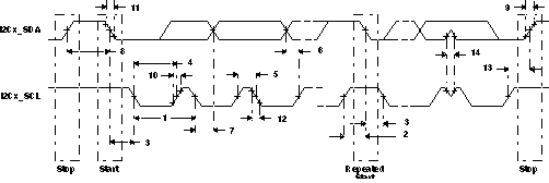 Figure 6-38 I2C Receive Timings
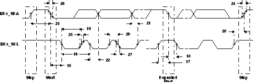 Figure 6-39 I2C Transmit Timings
6.17 Universal Asynchronous Receiver/Transmitter (UART)
Each UART has the following features:
- 16-byte storage space for both the transmitter and receiver FIFOs
- 1, 4, 8, or 14 byte selectable receiver FIFO trigger level for autoflow control and DMA
- DMA signaling capability for both received and transmitted data
- Programmable auto-rts and auto-cts for autoflow control
- Programmable Baud Rate up to 12 MBaud
- Programmable Oversampling Options of x13 and x16
- Frequency pre-scale values from 1 to 65,535 to generate appropriate baud rates
- Prioritized interrupts
- Programmable serial data formats
- 5, 6, 7, or 8-bit characters
- Even, odd, or no parity bit generation and detection
- 1, 1.5, or 2 stop bit generation
- False start bit detection
- Line break generation and detection
- Internal diagnostic capabilities
- Loopback controls for communications link fault isolation
- Break, parity, overrun, and framing error simulation
- Modem control functions (CTS, RTS)
The UART registers are listed in Section 6.17.1
6.17.1 UART Peripheral Registers Description(s)
Table 6-69 is the list of UART registers.
Table 6-69 UART Registers
| UART0 BYTE ADDRESS |
UART1 BYTE ADDRESS |
UART2 BYTE ADDRESS |
ACRONYM | REGISTER DESCRIPTION |
|---|---|---|---|---|
| 0x01C4 2000 | 0x01D0 C000 | 0x01D0 D000 | RBR | Receiver Buffer Register (read only) |
| 0x01C4 2000 | 0x01D0 C000 | 0x01D0 D000 | THR | Transmitter Holding Register (write only) |
| 0x01C4 2004 | 0x01D0 C004 | 0x01D0 D004 | IER | Interrupt Enable Register |
| 0x01C4 2008 | 0x01D0 C008 | 0x01D0 D008 | IIR | Interrupt Identification Register (read only) |
| 0x01C4 2008 | 0x01D0 C008 | 0x01D0 D008 | FCR | FIFO Control Register (write only) |
| 0x01C4 200C | 0x01D0 C00C | 0x01D0 D00C | LCR | Line Control Register |
| 0x01C4 2010 | 0x01D0 C010 | 0x01D0 D010 | MCR | Modem Control Register |
| 0x01C4 2014 | 0x01D0 C014 | 0x01D0 D014 | LSR | Line Status Register |
| 0x01C4 2018 | 0x01D0 C018 | 0x01D0 D018 | MSR | Modem Status Register |
| 0x01C4 201C | 0x01D0 C01C | 0x01D0 D01C | SCR | Scratchpad Register |
| 0x01C4 2020 | 0x01D0 C020 | 0x01D0 D020 | DLL | Divisor LSB Latch |
| 0x01C4 2024 | 0x01D0 C024 | 0x01D0 D024 | DLH | Divisor MSB Latch |
| 0x01C4 2028 | 0x01D0 C028 | 0x01D0 D028 | REVID1 | Revision Identification Register 1 |
| 0x01C4 2030 | 0x01D0 C030 | 0x01D0 D030 | PWREMU_MGMT | Power and Emulation Management Register |
| 0x01C4 2034 | 0x01D0 C034 | 0x01D0 D034 | MDR | Mode Definition Register |
6.17.2 UART Electrical Data/Timing
Table 6-70 Timing Requirements for UART Receive(1) (see Figure 6-40)
| NO. | 1.2V, 1.1V, 1.0V | UNIT | |||
|---|---|---|---|---|---|
| MIN | MAX | ||||
| 4 | tw(URXDB) | Pulse duration, receive data bit (RXDn) | 0.96U | 1.05U | ns |
| 5 | tw(URXSB) | Pulse duration, receive start bit | 0.96U | 1.05U | ns |
Table 6-71 Switching Characteristics Over Recommended Operating Conditions for UARTx Transmit(1)
(see Figure 6-40)
| NO. | PARAMETER | 1.2V, 1.1V, 1.0V | UNIT | ||
|---|---|---|---|---|---|
| MIN | MAX | ||||
| 1 | f(baud) | Maximum programmable baud rate | D/E (2)(3) | MBaud (4) | |
| 2 | tw(UTXDB) | Pulse duration, transmit data bit (TXDn) | U - 2 | U + 2 | ns |
| 3 | tw(UTXSB) | Pulse duration, transmit start bit | U - 2 | U + 2 | ns |
For UART0, the UART input clock is SYSCLK2.
For UART1 or UART2, the UART input clock is ASYNC3 (either PLL0_SYCLK2 or PLL1_SYSCLK2).
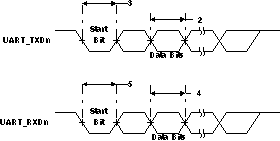 Figure 6-40 UART Transmit/Receive Timing
6.18 Universal Serial Bus OTG Controller (USB0) [USB2.0 OTG]
The USB2.0 peripheral supports the following features:
- USB 2.0 peripheral at speeds high speed (HS: 480 Mb/s) and full speed (FS: 12 Mb/s)
- USB 2.0 host at speeds HS, FS, and low speed (LS: 1.5 Mb/s)
- All transfer modes (control, bulk, interrupt, and isochronous)
- 4 Transmit (TX) and 4 Receive (RX) endpoints in addition to endpoint 0
- FIFO RAM
- 4K endpoint
- Programmable size
- Integrated USB 2.0 High Speed PHY
- Connects to a standard Charge Pump for VBUS 5 V generation
- RNDIS mode for accelerating RNDIS type protocols using short packet termination over USB
Important Notice: The USB0 controller module clock (PLL0_SYSCLK2) must be greater than 30 MHz for proper operation of the USB controller. A clock rate of 60 MHz or greater is recommended to avoid data throughput reduction.
Table 6-72 is the list of USB OTG registers.
Table 6-72 Universal Serial Bus OTG (USB0) Registers
| BYTE ADDRESS | ACRONYM | REGISTER DESCRIPTION |
|---|---|---|
| 0x01E0 0000 | REVID | Revision Register |
| 0x01E0 0004 | CTRLR | Control Register |
| 0x01E0 0008 | STATR | Status Register |
| 0x01E0 000C | EMUR | Emulation Register |
| 0x01E0 0010 | MODE | Mode Register |
| 0x01E0 0014 | AUTOREQ | Autorequest Register |
| 0x01E0 0018 | SRPFIXTIME | SRP Fix Time Register |
| 0x01E0 001C | TEARDOWN | Teardown Register |
| 0x01E0 0020 | INTSRCR | USB Interrupt Source Register |
| 0x01E0 0024 | INTSETR | USB Interrupt Source Set Register |
| 0x01E0 0028 | INTCLRR | USB Interrupt Source Clear Register |
| 0x01E0 002C | INTMSKR | USB Interrupt Mask Register |
| 0x01E0 0030 | INTMSKSETR | USB Interrupt Mask Set Register |
| 0x01E0 0034 | INTMSKCLRR | USB Interrupt Mask Clear Register |
| 0x01E0 0038 | INTMASKEDR | USB Interrupt Source Masked Register |
| 0x01E0 003C | EOIR | USB End of Interrupt Register |
| 0x01E0 0040 | - | Reserved |
| 0x01E0 0050 | GENRNDISSZ1 | Generic RNDIS Size EP1 |
| 0x01E0 0054 | GENRNDISSZ2 | Generic RNDIS Size EP2 |
| 0x01E0 0058 | GENRNDISSZ3 | Generic RNDIS Size EP3 |
| 0x01E0 005C | GENRNDISSZ4 | Generic RNDIS Size EP4 |
| 0x01E0 0400 | FADDR | Function Address Register |
| 0x01E0 0401 | POWER | Power Management Register |
| 0x01E0 0402 | INTRTX | Interrupt Register for Endpoint 0 plus Transmit Endpoints 1 to 4 |
| 0x01E0 0404 | INTRRX | Interrupt Register for Receive Endpoints 1 to 4 |
| 0x01E0 0406 | INTRTXE | Interrupt enable register for INTRTX |
| 0x01E0 0408 | INTRRXE | Interrupt Enable Register for INTRRX |
| 0x01E0 040A | INTRUSB | Interrupt Register for Common USB Interrupts |
| 0x01E0 040B | INTRUSBE | Interrupt Enable Register for INTRUSB |
| 0x01E0 040C | FRAME | Frame Number Register |
| 0x01E0 040E | INDEX | Index Register for Selecting the Endpoint Status and Control Registers |
| 0x01E0 040F | TESTMODE | Register to Enable the USB 2.0 Test Modes |
| Indexed Registers These registers operate on the endpoint selected by the INDEX register |
||
| 0x01E0 0410 | TXMAXP | Maximum Packet Size for Peripheral/Host Transmit Endpoint (Index register set to select Endpoints 1-4 only) |
| 0x01E0 0412 | PERI_CSR0 | Control Status Register for Endpoint 0 in Peripheral Mode. (Index register set to select Endpoint 0) |
| HOST_CSR0 | Control Status Register for Endpoint 0 in Host Mode. (Index register set to select Endpoint 0) |
|
| PERI_TXCSR | Control Status Register for Peripheral Transmit Endpoint. (Index register set to select Endpoints 1-4) |
|
| HOST_TXCSR | Control Status Register for Host Transmit Endpoint. (Index register set to select Endpoints 1-4) |
|
| 0x01E0 0414 | RXMAXP | Maximum Packet Size for Peripheral/Host Receive Endpoint (Index register set to select Endpoints 1-4 only) |
| 0x01E0 0416 | PERI_RXCSR | Control Status Register for Peripheral Receive Endpoint. (Index register set to select Endpoints 1-4) |
| HOST_RXCSR | Control Status Register for Host Receive Endpoint. (Index register set to select Endpoints 1-4) |
|
| 0x01E0 0418 | COUNT0 | Number of Received Bytes in Endpoint 0 FIFO. (Index register set to select Endpoint 0) |
| RXCOUNT | Number of Bytes in Host Receive Endpoint FIFO. (Index register set to select Endpoints 1- 4) |
|
| 0x01E0 041A | HOST_TYPE0 | Defines the speed of Endpoint 0 |
| HOST_TXTYPE | Sets the operating speed, transaction protocol and peripheral endpoint number for the host Transmit endpoint. (Index register set to select Endpoints 1-4 only) |
|
| 0x01E0 041B | HOST_NAKLIMIT0 | Sets the NAK response timeout on Endpoint 0. (Index register set to select Endpoint 0) |
| HOST_TXINTERVAL | Sets the polling interval for Interrupt/ISOC transactions or the NAK response timeout on Bulk transactions for host Transmit endpoint. (Index register set to select Endpoints 1-4 only) |
|
| 0x01E0 041C | HOST_RXTYPE | Sets the operating speed, transaction protocol and peripheral endpoint number for the host Receive endpoint. (Index register set to select Endpoints 1-4 only) |
| 0x01E0 041D | HOST_RXINTERVAL | Sets the polling interval for Interrupt/ISOC transactions or the NAK response timeout on Bulk transactions for host Receive endpoint. (Index register set to select Endpoints 1-4 only) |
| 0x01E0 041F | CONFIGDATA | Returns details of core configuration. (Index register set to select Endpoint 0) |
| FIFO | ||
| 0x01E0 0420 | FIFO0 | Transmit and Receive FIFO Register for Endpoint 0 |
| 0x01E0 0424 | FIFO1 | Transmit and Receive FIFO Register for Endpoint 1 |
| 0x01E0 0428 | FIFO2 | Transmit and Receive FIFO Register for Endpoint 2 |
| 0x01E0 042C | FIFO3 | Transmit and Receive FIFO Register for Endpoint 3 |
| 0x01E0 0430 | FIFO4 | Transmit and Receive FIFO Register for Endpoint 4 |
| OTG Device Control | ||
| 0x01E0 0460 | DEVCTL | Device Control Register |
| Dynamic FIFO Control | ||
| 0x01E0 0462 | TXFIFOSZ | Transmit Endpoint FIFO Size (Index register set to select Endpoints 1-4 only) |
| 0x01E0 0463 | RXFIFOSZ | Receive Endpoint FIFO Size (Index register set to select Endpoints 1-4 only) |
| 0x01E0 0464 | TXFIFOADDR | Transmit Endpoint FIFO Address (Index register set to select Endpoints 1-4 only) |
| 0x01E0 0466 | RXFIFOADDR | Receive Endpoint FIFO Address (Index register set to select Endpoints 1-4 only) |
| 0x01E0 046C | HWVERS | Hardware Version Register |
| Target Endpoint 0 Control Registers, Valid Only in Host Mode | ||
| 0x01E0 0480 | TXFUNCADDR | Address of the target function that has to be accessed through the associated Transmit Endpoint. |
| 0x01E0 0482 | TXHUBADDR | Address of the hub that has to be accessed through the associated Transmit Endpoint. This is used only when full speed or low speed device is connected via a USB2.0 high-speed hub. |
| 0x01E0 0483 | TXHUBPORT | Port of the hub that has to be accessed through the associated Transmit Endpoint. This is used only when full speed or low speed device is connected via a USB2.0 high-speed hub. |
| 0x01E0 0484 | RXFUNCADDR | Address of the target function that has to be accessed through the associated Receive Endpoint. |
| 0x01E0 0486 | RXHUBADDR | Address of the hub that has to be accessed through the associated Receive Endpoint. This is used only when full speed or low speed device is connected via a USB2.0 high-speed hub. |
| 0x01E0 0487 | RXHUBPORT | Port of the hub that has to be accessed through the associated Receive Endpoint. This is used only when full speed or low speed device is connected via a USB2.0 high-speed hub. |
| Target Endpoint 1 Control Registers, Valid Only in Host Mode | ||
| 0x01E0 0488 | TXFUNCADDR | Address of the target function that has to be accessed through the associated Transmit Endpoint. |
| 0x01E0 048A | TXHUBADDR | Address of the hub that has to be accessed through the associated Transmit Endpoint. This is used only when full speed or low speed device is connected via a USB2.0 high-speed hub. |
| 0x01E0 048B | TXHUBPORT | Port of the hub that has to be accessed through the associated Transmit Endpoint. This is used only when full speed or low speed device is connected via a USB2.0 high-speed hub. |
| 0x01E0 048C | RXFUNCADDR | Address of the target function that has to be accessed through the associated Receive Endpoint. |
| 0x01E0 048E | RXHUBADDR | Address of the hub that has to be accessed through the associated Receive Endpoint. This is used only when full speed or low speed device is connected via a USB2.0 high-speed hub. |
| 0x01E0 048F | RXHUBPORT | Port of the hub that has to be accessed through the associated Receive Endpoint. This is used only when full speed or low speed device is connected via a USB2.0 high-speed hub. |
| Target Endpoint 2 Control Registers, Valid Only in Host Mode | ||
| 0x01E0 0490 | TXFUNCADDR | Address of the target function that has to be accessed through the associated Transmit Endpoint. |
| 0x01E0 0492 | TXHUBADDR | Address of the hub that has to be accessed through the associated Transmit Endpoint. This is used only when full speed or low speed device is connected via a USB2.0 high-speed hub. |
| 0x01E0 0493 | TXHUBPORT | Port of the hub that has to be accessed through the associated Transmit Endpoint. This is used only when full speed or low speed device is connected via a USB2.0 high-speed hub. |
| 0x01E0 0494 | RXFUNCADDR | Address of the target function that has to be accessed through the associated Receive Endpoint. |
| 0x01E0 0496 | RXHUBADDR | Address of the hub that has to be accessed through the associated Receive Endpoint. This is used only when full speed or low speed device is connected via a USB2.0 high-speed hub. |
| 0x01E0 0497 | RXHUBPORT | Port of the hub that has to be accessed through the associated Receive Endpoint. This is used only when full speed or low speed device is connected via a USB2.0 high-speed hub. |
| Target Endpoint 3 Control Registers, Valid Only in Host Mode | ||
| 0x01E0 0498 | TXFUNCADDR | Address of the target function that has to be accessed through the associated Transmit Endpoint. |
| 0x01E0 049A | TXHUBADDR | Address of the hub that has to be accessed through the associated Transmit Endpoint. This is used only when full speed or low speed device is connected via a USB2.0 high-speed hub. |
| 0x01E0 049B | TXHUBPORT | Port of the hub that has to be accessed through the associated Transmit Endpoint. This is used only when full speed or low speed device is connected via a USB2.0 high-speed hub. |
| 0x01E0 049C | RXFUNCADDR | Address of the target function that has to be accessed through the associated Receive Endpoint. |
| 0x01E0 049E | RXHUBADDR | Address of the hub that has to be accessed through the associated Receive Endpoint. This is used only when full speed or low speed device is connected via a USB2.0 high-speed hub. |
| 0x01E0 049F | RXHUBPORT | Port of the hub that has to be accessed through the associated Receive Endpoint. This is used only when full speed or low speed device is connected via a USB2.0 high-speed hub. |
| Target Endpoint 4 Control Registers, Valid Only in Host Mode | ||
| 0x01E0 04A0 | TXFUNCADDR | Address of the target function that has to be accessed through the associated Transmit Endpoint. |
| 0x01E0 04A2 | TXHUBADDR | Address of the hub that has to be accessed through the associated Transmit Endpoint. This is used only when full speed or low speed device is connected via a USB2.0 high-speed hub. |
| 0x01E0 04A3 | TXHUBPORT | Port of the hub that has to be accessed through the associated Transmit Endpoint. This is used only when full speed or low speed device is connected via a USB2.0 high-speed hub. |
| 0x01E0 04A4 | RXFUNCADDR | Address of the target function that has to be accessed through the associated Receive Endpoint. |
| 0x01E0 04A6 | RXHUBADDR | Address of the hub that has to be accessed through the associated Receive Endpoint. This is used only when full speed or low speed device is connected via a USB2.0 high-speed hub. |
| 0x01E0 04A7 | RXHUBPORT | Port of the hub that has to be accessed through the associated Receive Endpoint. This is used only when full speed or low speed device is connected via a USB2.0 high-speed hub. |
| Control and Status Register for Endpoint 0 | ||
| 0x01E0 0502 | PERI_CSR0 | Control Status Register for Endpoint 0 in Peripheral Mode |
| HOST_CSR0 | Control Status Register for Endpoint 0 in Host Mode | |
| 0x01E0 0508 | COUNT0 | Number of Received Bytes in Endpoint 0 FIFO |
| 0x01E0 050A | HOST_TYPE0 | Defines the Speed of Endpoint 0 |
| 0x01E0 050B | HOST_NAKLIMIT0 | Sets the NAK Response Timeout on Endpoint 0 |
| 0x01E0 050F | CONFIGDATA | Returns details of core configuration. |
| Control and Status Register for Endpoint 1 | ||
| 0x01E0 0510 | TXMAXP | Maximum Packet Size for Peripheral/Host Transmit Endpoint |
| 0x01E0 0512 | PERI_TXCSR | Control Status Register for Peripheral Transmit Endpoint (peripheral mode) |
| HOST_TXCSR | Control Status Register for Host Transmit Endpoint (host mode) | |
| 0x01E0 0514 | RXMAXP | Maximum Packet Size for Peripheral/Host Receive Endpoint |
| 0x01E0 0516 | PERI_RXCSR | Control Status Register for Peripheral Receive Endpoint (peripheral mode) |
| HOST_RXCSR | Control Status Register for Host Receive Endpoint (host mode) | |
| 0x01E0 0518 | RXCOUNT | Number of Bytes in Host Receive endpoint FIFO |
| 0x01E0 051A | HOST_TXTYPE | Sets the operating speed, transaction protocol and peripheral endpoint number for the host Transmit endpoint. |
| 0x01E0 051B | HOST_TXINTERVAL | Sets the polling interval for Interrupt/ISOC transactions or the NAK response timeout on Bulk transactions for host Transmit endpoint. |
| 0x01E0 051C | HOST_RXTYPE | Sets the operating speed, transaction protocol and peripheral endpoint number for the host Receive endpoint. |
| 0x01E0 051D | HOST_RXINTERVAL | Sets the polling interval for Interrupt/ISOC transactions or the NAK response timeout on Bulk transactions for host Receive endpoint. |
| Control and Status Register for Endpoint 2 | ||
| 0x01E0 0520 | TXMAXP | Maximum Packet Size for Peripheral/Host Transmit Endpoint |
| 0x01E0 0522 | PERI_TXCSR | Control Status Register for Peripheral Transmit Endpoint (peripheral mode) |
| HOST_TXCSR | Control Status Register for Host Transmit Endpoint (host mode) | |
| 0x01E0 0524 | RXMAXP | Maximum Packet Size for Peripheral/Host Receive Endpoint |
| 0x01E0 0526 | PERI_RXCSR | Control Status Register for Peripheral Receive Endpoint (peripheral mode) |
| HOST_RXCSR | Control Status Register for Host Receive Endpoint (host mode) | |
| 0x01E0 0528 | RXCOUNT | Number of Bytes in Host Receive endpoint FIFO |
| 0x01E0 052A | HOST_TXTYPE | Sets the operating speed, transaction protocol and peripheral endpoint number for the host Transmit endpoint. |
| 0x01E0 052B | HOST_TXINTERVAL | Sets the polling interval for Interrupt/ISOC transactions or the NAK response timeout on Bulk transactions for host Transmit endpoint. |
| 0x01E0 052C | HOST_RXTYPE | Sets the operating speed, transaction protocol and peripheral endpoint number for the host Receive endpoint. |
| 0x01E0 052D | HOST_RXINTERVAL | Sets the polling interval for Interrupt/ISOC transactions or the NAK response timeout on Bulk transactions for host Receive endpoint. |
| Control and Status Register for Endpoint 3 | ||
| 0x01E0 0530 | TXMAXP | Maximum Packet Size for Peripheral/Host Transmit Endpoint |
| 0x01E0 0532 | PERI_TXCSR | Control Status Register for Peripheral Transmit Endpoint (peripheral mode) |
| HOST_TXCSR | Control Status Register for Host Transmit Endpoint (host mode) | |
| 0x01E0 0534 | RXMAXP | Maximum Packet Size for Peripheral/Host Receive Endpoint |
| 0x01E0 0536 | PERI_RXCSR | Control Status Register for Peripheral Receive Endpoint (peripheral mode) |
| HOST_RXCSR | Control Status Register for Host Receive Endpoint (host mode) | |
| 0x01E0 0538 | RXCOUNT | Number of Bytes in Host Receive endpoint FIFO |
| 0x01E0 053A | HOST_TXTYPE | Sets the operating speed, transaction protocol and peripheral endpoint number for the host Transmit endpoint. |
| 0x01E0 053B | HOST_TXINTERVAL | Sets the polling interval for Interrupt/ISOC transactions or the NAK response timeout on Bulk transactions for host Transmit endpoint. |
| 0x01E0 053C | HOST_RXTYPE | Sets the operating speed, transaction protocol and peripheral endpoint number for the host Receive endpoint. |
| 0x01E0 053D | HOST_RXINTERVAL | Sets the polling interval for Interrupt/ISOC transactions or the NAK response timeout on Bulk transactions for host Receive endpoint. |
| Control and Status Register for Endpoint 4 | ||
| 0x01E0 0540 | TXMAXP | Maximum Packet Size for Peripheral/Host Transmit Endpoint |
| 0x01E0 0542 | PERI_TXCSR | Control Status Register for Peripheral Transmit Endpoint (peripheral mode) |
| HOST_TXCSR | Control Status Register for Host Transmit Endpoint (host mode) | |
| 0x01E0 0544 | RXMAXP | Maximum Packet Size for Peripheral/Host Receive Endpoint |
| 0x01E0 0546 | PERI_RXCSR | Control Status Register for Peripheral Receive Endpoint (peripheral mode) |
| HOST_RXCSR | Control Status Register for Host Receive Endpoint (host mode) | |
| 0x01E0 0548 | RXCOUNT | Number of Bytes in Host Receive endpoint FIFO |
| 0x01E0 054A | HOST_TXTYPE | Sets the operating speed, transaction protocol and peripheral endpoint number for the host Transmit endpoint. |
| 0x01E0 054B | HOST_TXINTERVAL | Sets the polling interval for Interrupt/ISOC transactions or the NAK response timeout on Bulk transactions for host Transmit endpoint. |
| 0x01E0 054C | HOST_RXTYPE | Sets the operating speed, transaction protocol and peripheral endpoint number for the host Receive endpoint. |
| 0x01E0 054D | HOST_RXINTERVAL | Sets the polling interval for Interrupt/ISOC transactions or the NAK response timeout on Bulk transactions for host Receive endpoint. |
| DMA Registers | ||
| 0x01E0 1000 | DMAREVID | DMA Revision Register |
| 0x01E0 1004 | TDFDQ | DMA Teardown Free Descriptor Queue Control Register |
| 0x01E0 1008 | DMAEMU | DMA Emulation Control Register |
| 0x01E0 1800 | TXGCR[0] | Transmit Channel 0 Global Configuration Register |
| 0x01E0 1808 | RXGCR[0] | Receive Channel 0 Global Configuration Register |
| 0x01E0 180C | RXHPCRA[0] | Receive Channel 0 Host Packet Configuration Register A |
| 0x01E0 1810 | RXHPCRB[0] | Receive Channel 0 Host Packet Configuration Register B |
| 0x01E0 1820 | TXGCR[1] | Transmit Channel 1 Global Configuration Register |
| 0x01E0 1828 | RXGCR[1] | Receive Channel 1 Global Configuration Register |
| 0x01E0 182C | RXHPCRA[1] | Receive Channel 1 Host Packet Configuration Register A |
| 0x01E0 1830 | RXHPCRB[1] | Receive Channel 1 Host Packet Configuration Register B |
| 0x01E0 1840 | TXGCR[2] | Transmit Channel 2 Global Configuration Register |
| 0x01E0 1848 | RXGCR[2] | Receive Channel 2 Global Configuration Register |
| 0x01E0 184C | RXHPCRA[2] | Receive Channel 2 Host Packet Configuration Register A |
| 0x01E0 1850 | RXHPCRB[2] | Receive Channel 2 Host Packet Configuration Register B |
| 0x01E0 1860 | TXGCR[3] | Transmit Channel 3 Global Configuration Register |
| 0x01E0 1868 | RXGCR[3] | Receive Channel 3 Global Configuration Register |
| 0x01E0 186C | RXHPCRA[3] | Receive Channel 3 Host Packet Configuration Register A |
| 0x01E0 1870 | RXHPCRB[3] | Receive Channel 3 Host Packet Configuration Register B |
| 0x01E0 2000 | DMA_SCHED_CTRL | DMA Scheduler Control Register |
| 0x01E0 2800 | WORD[0] | DMA Scheduler Table Word 0 |
| 0x01E0 2804 | WORD[1] | DMA Scheduler Table Word 1 |
| . . . | . . . | . . . |
| 0x01E0 28FC | WORD[63] | DMA Scheduler Table Word 63 |
| Queue Manager Registers | ||
| 0x01E0 4000 | QMGRREVID | Queue Manager Revision Register |
| 0x01E0 4008 | DIVERSION | Queue Diversion Register |
| 0x01E0 4020 | FDBSC0 | Free Descriptor/Buffer Starvation Count Register 0 |
| 0x01E0 4024 | FDBSC1 | Free Descriptor/Buffer Starvation Count Register 1 |
| 0x01E0 4028 | FDBSC2 | Free Descriptor/Buffer Starvation Count Register 2 |
| 0x01E0 402C | FDBSC3 | Free Descriptor/Buffer Starvation Count Register 3 |
| 0x01E0 4080 | LRAM0BASE | Linking RAM Region 0 Base Address Register |
| 0x01E0 4084 | LRAM0SIZE | Linking RAM Region 0 Size Register |
| 0x01E0 4088 | LRAM1BASE | Linking RAM Region 1 Base Address Register |
| 0x01E0 4090 | PEND0 | Queue Pending Register 0 |
| 0x01E0 4094 | PEND1 | Queue Pending Register 1 |
| 0x01E0 5000 | QMEMRBASE[0] | Memory Region 0 Base Address Register |
| 0x01E0 5004 | QMEMRCTRL[0] | Memory Region 0 Control Register |
| 0x01E0 5010 | QMEMRBASE[1] | Memory Region 1 Base Address Register |
| 0x01E0 5014 | QMEMRCTRL[1] | Memory Region 1 Control Register |
| . . . | . . . | . . . |
| 0x01E0 50F0 | QMEMRBASE[15] | Memory Region 15 Base Address Register |
| 0x01E0 50F4 | QMEMRCTRL[15] | Memory Region 15 Control Register |
| 0x01E0 600C | CTRLD[0] | Queue Manager Queue 0 Control Register D |
| 0x01E0 601C | CTRLD[1] | Queue Manager Queue 1 Control Register D |
| . . . | . . . | . . . |
| 0x01E0 63FC | CTRLD[63] | Queue Manager Queue 63 Status Register D |
| 0x01E0 6800 | QSTATA[0] | Queue Manager Queue 0 Status Register A |
| 0x01E0 6804 | QSTATB[0] | Queue Manager Queue 0 Status Register B |
| 0x01E0 6808 | QSTATC[0] | Queue Manager Queue 0 Status Register C |
| 0x01E0 6810 | QSTATA[1] | Queue Manager Queue 1 Status Register A |
| 0x01E0 6814 | QSTATB[1] | Queue Manager Queue 1 Status Register B |
| 0x01E0 6818 | QSTATC[1] | Queue Manager Queue 1 Status Register C |
| . . . | . . . | . . . |
| 0x01E0 6BF0 | QSTATA[63] | Queue Manager Queue 63 Status Register A |
| 0x01E0 6BF4 | QSTATB[63] | Queue Manager Queue 63 Status Register B |
| 0x01E0 6BF8 | QSTATC[63] | Queue Manager Queue 63 Status Register C |
6.18.1 USB0 [USB2.0] Electrical Data/Timing
The USB PHY PLL can support input clock of the following frequencies: 12.0 MHz, 13.0 MHz, 19.2 MHz, 20.0 MHz, 24.0 MHz, 26.0 MHz, 38.4 MHz, 40.0 MHz or 48.0 MHz. USB_REFCLKIN jitter tolerance is 50 ppm maximum.
Table 6-73 Switching Characteristics Over Recommended Operating Conditions for USB0 [USB2.0] (see Figure 6-41)
| NO. | PARAMETER | 1.2V, 1.1V, 1.0V | UNIT | ||||||
|---|---|---|---|---|---|---|---|---|---|
| LOW SPEED 1.5 Mbps |
FULL SPEED 12 Mbps |
HIGH SPEED 480 Mbps |
|||||||
| MIN | MAX | MIN | MAX | MIN | MAX | ||||
| 1 | tr(D) | Rise time, USB_DP and USB_DM signals(1) | 75 | 300 | 4 | 20 | 0.5 | ns | |
| 2 | tf(D) | Fall time, USB_DP and USB_DM signals(1) | 75 | 300 | 4 | 20 | 0.5 | ns | |
| 3 | trfM | Rise/Fall time, matching(2) | 80 | 120 | 90 | 111 | - | - | % |
| 4 | VCRS | Output signal cross-over voltage(1) | 1.3 | 2 | 1.3 | 2 | - | - | V |
| 5 | tjr(source)NT | Source (Host) Driver jitter, next transition | 2 | 2 | (4) | ns | |||
| tjr(FUNC)NT | Function Driver jitter, next transition | 25 | 2 | (4) | ns | ||||
| 6 | tjr(source)PT | Source (Host) Driver jitter, paired transition(3) | 1 | 1 | (4) | ns | |||
| tjr(FUNC)PT | Function Driver jitter, paired transition | 10 | 1 | (4) | ns | ||||
| 7 | tw(EOPT) | Pulse duration, EOP transmitter | 1250 | 1500 | 160 | 175 | - | - | ns |
| 8 | tw(EOPR) | Pulse duration, EOP receiver | 670 | 82 | - | ns | |||
| 9 | t(DRATE) | Data Rate | 1.5 | 12 | 480 | Mb/s | |||
| 10 | ZDRV | Driver Output Resistance | - | - | 40.5 | 49.5 | 40.5 | 49.5 | Ω |
| 11 | ZINP | Receiver Input Impedance | 100k | 100k | - | - | Ω | ||
 Figure 6-41 USB2.0 Integrated Transceiver Interface Timing
6.19 Ethernet Media Access Controller (EMAC)
The Ethernet Media Access Controller (EMAC) provides an efficient interface between device and the network. The EMAC supports both 10Base-T and 100Base-TX, or 10 Mbits/second (Mbps) and 100 Mbps in either half- or full-duplex mode, with hardware flow control and quality of service (QOS) support.
The EMAC controls the flow of packet data from the device to the PHY. The MDIO module controls PHY configuration and status monitoring.
Both the EMAC and the MDIO modules interface to the device through a custom interface that allows efficient data transmission and reception. This custom interface is referred to as the EMAC control module, and is considered integral to the EMAC/MDIO peripheral. The control module is also used to multiplex and control interrupts.
6.19.1 EMAC Peripheral Register Description(s)
Table 6-74 Ethernet Media Access Controller (EMAC) Registers
| BYTE ADDRESS | ACRONYM | REGISTER DESCRIPTION |
|---|---|---|
| 0x01E2 3000 | TXREV | Transmit Revision Register |
| 0x01E2 3004 | TXCONTROL | Transmit Control Register |
| 0x01E2 3008 | TXTEARDOWN | Transmit Teardown Register |
| 0x01E2 3010 | RXREV | Receive Revision Register |
| 0x01E2 3014 | RXCONTROL | Receive Control Register |
| 0x01E2 3018 | RXTEARDOWN | Receive Teardown Register |
| 0x01E2 3080 | TXINTSTATRAW | Transmit Interrupt Status (Unmasked) Register |
| 0x01E2 3084 | TXINTSTATMASKED | Transmit Interrupt Status (Masked) Register |
| 0x01E2 3088 | TXINTMASKSET | Transmit Interrupt Mask Set Register |
| 0x01E2 308C | TXINTMASKCLEAR | Transmit Interrupt Clear Register |
| 0x01E2 3090 | MACINVECTOR | MAC Input Vector Register |
| 0x01E2 3094 | MACEOIVECTOR | MAC End Of Interrupt Vector Register |
| 0x01E2 30A0 | RXINTSTATRAW | Receive Interrupt Status (Unmasked) Register |
| 0x01E2 30A4 | RXINTSTATMASKED | Receive Interrupt Status (Masked) Register |
| 0x01E2 30A8 | RXINTMASKSET | Receive Interrupt Mask Set Register |
| 0x01E2 30AC | RXINTMASKCLEAR | Receive Interrupt Mask Clear Register |
| 0x01E2 30B0 | MACINTSTATRAW | MAC Interrupt Status (Unmasked) Register |
| 0x01E2 30B4 | MACINTSTATMASKED | MAC Interrupt Status (Masked) Register |
| 0x01E2 30B8 | MACINTMASKSET | MAC Interrupt Mask Set Register |
| 0x01E2 30BC | MACINTMASKCLEAR | MAC Interrupt Mask Clear Register |
| 0x01E2 3100 | RXMBPENABLE | Receive Multicast/Broadcast/Promiscuous Channel Enable Register |
| 0x01E2 3104 | RXUNICASTSET | Receive Unicast Enable Set Register |
| 0x01E2 3108 | RXUNICASTCLEAR | Receive Unicast Clear Register |
| 0x01E2 310C | RXMAXLEN | Receive Maximum Length Register |
| 0x01E2 3110 | RXBUFFEROFFSET | Receive Buffer Offset Register |
| 0x01E2 3114 | RXFILTERLOWTHRESH | Receive Filter Low Priority Frame Threshold Register |
| 0x01E2 3120 | RX0FLOWTHRESH | Receive Channel 0 Flow Control Threshold Register |
| 0x01E2 3124 | RX1FLOWTHRESH | Receive Channel 1 Flow Control Threshold Register |
| 0x01E2 3128 | RX2FLOWTHRESH | Receive Channel 2 Flow Control Threshold Register |
| 0x01E2 312C | RX3FLOWTHRESH | Receive Channel 3 Flow Control Threshold Register |
| 0x01E2 3130 | RX4FLOWTHRESH | Receive Channel 4 Flow Control Threshold Register |
| 0x01E2 3134 | RX5FLOWTHRESH | Receive Channel 5 Flow Control Threshold Register |
| 0x01E2 3138 | RX6FLOWTHRESH | Receive Channel 6 Flow Control Threshold Register |
| 0x01E2 313C | RX7FLOWTHRESH | Receive Channel 7 Flow Control Threshold Register |
| 0x01E2 3140 | RX0FREEBUFFER | Receive Channel 0 Free Buffer Count Register |
| 0x01E2 3144 | RX1FREEBUFFER | Receive Channel 1 Free Buffer Count Register |
| 0x01E2 3148 | RX2FREEBUFFER | Receive Channel 2 Free Buffer Count Register |
| 0x01E2 314C | RX3FREEBUFFER | Receive Channel 3 Free Buffer Count Register |
| 0x01E2 3150 | RX4FREEBUFFER | Receive Channel 4 Free Buffer Count Register |
| 0x01E2 3154 | RX5FREEBUFFER | Receive Channel 5 Free Buffer Count Register |
| 0x01E2 3158 | RX6FREEBUFFER | Receive Channel 6 Free Buffer Count Register |
| 0x01E2 315C | RX7FREEBUFFER | Receive Channel 7 Free Buffer Count Register |
| 0x01E2 3160 | MACCONTROL | MAC Control Register |
| 0x01E2 3164 | MACSTATUS | MAC Status Register |
| 0x01E2 3168 | EMCONTROL | Emulation Control Register |
| 0x01E2 316C | FIFOCONTROL | FIFO Control Register |
| 0x01E2 3170 | MACCONFIG | MAC Configuration Register |
| 0x01E2 3174 | SOFTRESET | Soft Reset Register |
| 0x01E2 31D0 | MACSRCADDRLO | MAC Source Address Low Bytes Register |
| 0x01E2 31D4 | MACSRCADDRHI | MAC Source Address High Bytes Register |
| 0x01E2 31D8 | MACHASH1 | MAC Hash Address Register 1 |
| 0x01E2 31DC | MACHASH2 | MAC Hash Address Register 2 |
| 0x01E2 31E0 | BOFFTEST | Back Off Test Register |
| 0x01E2 31E4 | TPACETEST | Transmit Pacing Algorithm Test Register |
| 0x01E2 31E8 | RXPAUSE | Receive Pause Timer Register |
| 0x01E2 31EC | TXPAUSE | Transmit Pause Timer Register |
| 0x01E2 3200 - 0x01E2 32FC | (see Table 6-75) | EMAC Statistics Registers |
| 0x01E2 3500 | MACADDRLO | MAC Address Low Bytes Register, Used in Receive Address Matching |
| 0x01E2 3504 | MACADDRHI | MAC Address High Bytes Register, Used in Receive Address Matching |
| 0x01E2 3508 | MACINDEX | MAC Index Register |
| 0x01E2 3600 | TX0HDP | Transmit Channel 0 DMA Head Descriptor Pointer Register |
| 0x01E2 3604 | TX1HDP | Transmit Channel 1 DMA Head Descriptor Pointer Register |
| 0x01E2 3608 | TX2HDP | Transmit Channel 2 DMA Head Descriptor Pointer Register |
| 0x01E2 360C | TX3HDP | Transmit Channel 3 DMA Head Descriptor Pointer Register |
| 0x01E2 3610 | TX4HDP | Transmit Channel 4 DMA Head Descriptor Pointer Register |
| 0x01E2 3614 | TX5HDP | Transmit Channel 5 DMA Head Descriptor Pointer Register |
| 0x01E2 3618 | TX6HDP | Transmit Channel 6 DMA Head Descriptor Pointer Register |
| 0x01E2 361C | TX7HDP | Transmit Channel 7 DMA Head Descriptor Pointer Register |
| 0x01E2 3620 | RX0HDP | Receive Channel 0 DMA Head Descriptor Pointer Register |
| 0x01E2 3624 | RX1HDP | Receive Channel 1 DMA Head Descriptor Pointer Register |
| 0x01E2 3628 | RX2HDP | Receive Channel 2 DMA Head Descriptor Pointer Register |
| 0x01E2 362C | RX3HDP | Receive Channel 3 DMA Head Descriptor Pointer Register |
| 0x01E2 3630 | RX4HDP | Receive Channel 4 DMA Head Descriptor Pointer Register |
| 0x01E2 3634 | RX5HDP | Receive Channel 5 DMA Head Descriptor Pointer Register |
| 0x01E2 3638 | RX6HDP | Receive Channel 6 DMA Head Descriptor Pointer Register |
| 0x01E2 363C | RX7HDP | Receive Channel 7 DMA Head Descriptor Pointer Register |
| 0x01E2 3640 | TX0CP | Transmit Channel 0 Completion Pointer Register |
| 0x01E2 3644 | TX1CP | Transmit Channel 1 Completion Pointer Register |
| 0x01E2 3648 | TX2CP | Transmit Channel 2 Completion Pointer Register |
| 0x01E2 364C | TX3CP | Transmit Channel 3 Completion Pointer Register |
| 0x01E2 3650 | TX4CP | Transmit Channel 4 Completion Pointer Register |
| 0x01E2 3654 | TX5CP | Transmit Channel 5 Completion Pointer Register |
| 0x01E2 3658 | TX6CP | Transmit Channel 6 Completion Pointer Register |
| 0x01E2 365C | TX7CP | Transmit Channel 7 Completion Pointer Register |
| 0x01E2 3660 | RX0CP | Receive Channel 0 Completion Pointer Register |
| 0x01E2 3664 | RX1CP | Receive Channel 1 Completion Pointer Register |
| 0x01E2 3668 | RX2CP | Receive Channel 2 Completion Pointer Register |
| 0x01E2 366C | RX3CP | Receive Channel 3 Completion Pointer Register |
| 0x01E2 3670 | RX4CP | Receive Channel 4 Completion Pointer Register |
| 0x01E2 3674 | RX5CP | Receive Channel 5 Completion Pointer Register |
| 0x01E2 3678 | RX6CP | Receive Channel 6 Completion Pointer Register |
| 0x01E2 367C | RX7CP | Receive Channel 7 Completion Pointer Register |
Table 6-75 EMAC Statistics Registers
| BYTE ADDRESS | ACRONYM | REGISTER DESCRIPTION |
|---|---|---|
| 0x01E2 3200 | RXGOODFRAMES | Good Receive Frames Register |
| 0x01E2 3204 | RXBCASTFRAMES | Broadcast Receive Frames Register (Total number of good broadcast frames received) |
| 0x01E2 3208 | RXMCASTFRAMES | Multicast Receive Frames Register (Total number of good multicast frames received) |
| 0x01E2 320C | RXPAUSEFRAMES | Pause Receive Frames Register |
| 0x01E2 3210 | RXCRCERRORS | Receive CRC Errors Register (Total number of frames received with CRC errors) |
| 0x01E2 3214 | RXALIGNCODEERRORS | Receive Alignment/Code Errors Register (Total number of frames received with alignment/code errors) |
| 0x01E2 3218 | RXOVERSIZED | Receive Oversized Frames Register (Total number of oversized frames received) |
| 0x01E2 321C | RXJABBER | Receive Jabber Frames Register (Total number of jabber frames received) |
| 0x01E2 3220 | RXUNDERSIZED | Receive Undersized Frames Register (Total number of undersized frames received) |
| 0x01E2 3224 | RXFRAGMENTS | Receive Frame Fragments Register |
| 0x01E2 3228 | RXFILTERED | Filtered Receive Frames Register |
| 0x01E2 322C | RXQOSFILTERED | Received QOS Filtered Frames Register |
| 0x01E2 3230 | RXOCTETS | Receive Octet Frames Register (Total number of received bytes in good frames) |
| 0x01E2 3234 | TXGOODFRAMES | Good Transmit Frames Register (Total number of good frames transmitted) |
| 0x01E2 3238 | TXBCASTFRAMES | Broadcast Transmit Frames Register |
| 0x01E2 323C | TXMCASTFRAMES | Multicast Transmit Frames Register |
| 0x01E2 3240 | TXPAUSEFRAMES | Pause Transmit Frames Register |
| 0x01E2 3244 | TXDEFERRED | Deferred Transmit Frames Register |
| 0x01E2 3248 | TXCOLLISION | Transmit Collision Frames Register |
| 0x01E2 324C | TXSINGLECOLL | Transmit Single Collision Frames Register |
| 0x01E2 3250 | TXMULTICOLL | Transmit Multiple Collision Frames Register |
| 0x01E2 3254 | TXEXCESSIVECOLL | Transmit Excessive Collision Frames Register |
| 0x01E2 3258 | TXLATECOLL | Transmit Late Collision Frames Register |
| 0x01E2 325C | TXUNDERRUN | Transmit Underrun Error Register |
| 0x01E2 3260 | TXCARRIERSENSE | Transmit Carrier Sense Errors Register |
| 0x01E2 3264 | TXOCTETS | Transmit Octet Frames Register |
| 0x01E2 3268 | FRAME64 | Transmit and Receive 64 Octet Frames Register |
| 0x01E2 326C | FRAME65T127 | Transmit and Receive 65 to 127 Octet Frames Register |
| 0x01E2 3270 | FRAME128T255 | Transmit and Receive 128 to 255 Octet Frames Register |
| 0x01E2 3274 | FRAME256T511 | Transmit and Receive 256 to 511 Octet Frames Register |
| 0x01E2 3278 | FRAME512T1023 | Transmit and Receive 512 to 1023 Octet Frames Register |
| 0x01E2 327C | FRAME1024TUP | Transmit and Receive 1024 to 1518 Octet Frames Register |
| 0x01E2 3280 | NETOCTETS | Network Octet Frames Register |
| 0x01E2 3284 | RXSOFOVERRUNS | Receive FIFO or DMA Start of Frame Overruns Register |
| 0x01E2 3288 | RXMOFOVERRUNS | Receive FIFO or DMA Middle of Frame Overruns Register |
| 0x01E2 328C | RXDMAOVERRUNS | Receive DMA Start of Frame and Middle of Frame Overruns Register |
Table 6-76 EMAC Control Module Registers
| BYTE ADDRESS | ACRONYM | REGISTER DESCRIPTION |
|---|---|---|
| 0x01E2 2000 | REV | EMAC Control Module Revision Register |
| 0x01E2 2004 | SOFTRESET | EMAC Control Module Software Reset Register |
| 0x01E2 200C | INTCONTROL | EMAC Control Module Interrupt Control Register |
| 0x01E2 2010 | C0RXTHRESHEN | EMAC Control Module Interrupt Core 0 Receive Threshold Interrupt Enable Register |
| 0x01E2 2014 | C0RXEN | EMAC Control Module Interrupt Core 0 Receive Interrupt Enable Register |
| 0x01E2 2018 | C0TXEN | EMAC Control Module Interrupt Core 0 Transmit Interrupt Enable Register |
| 0x01E2 201C | C0MISCEN | EMAC Control Module Interrupt Core 0 Miscellaneous Interrupt Enable Register |
| 0x01E2 2020 | C1RXTHRESHEN | EMAC Control Module Interrupt Core 1 Receive Threshold Interrupt Enable Register |
| 0x01E2 2024 | C1RXEN | EMAC Control Module Interrupt Core 1 Receive Interrupt Enable Register |
| 0x01E2 2028 | C1TXEN | EMAC Control Module Interrupt Core 1 Transmit Interrupt Enable Register |
| 0x01E2 202C | C1MISCEN | EMAC Control Module Interrupt Core 1 Miscellaneous Interrupt Enable Register |
| 0x01E2 2030 | C2RXTHRESHEN | EMAC Control Module Interrupt Core 2 Receive Threshold Interrupt Enable Register |
| 0x01E2 2034 | C2RXEN | EMAC Control Module Interrupt Core 2 Receive Interrupt Enable Register |
| 0x01E2 2038 | C2TXEN | EMAC Control Module Interrupt Core 2 Transmit Interrupt Enable Register |
| 0x01E2 203C | C2MISCEN | EMAC Control Module Interrupt Core 2 Miscellaneous Interrupt Enable Register |
| 0x01E2 2040 | C0RXTHRESHSTAT | EMAC Control Module Interrupt Core 0 Receive Threshold Interrupt Status Register |
| 0x01E2 2044 | C0RXSTAT | EMAC Control Module Interrupt Core 0 Receive Interrupt Status Register |
| 0x01E2 2048 | C0TXSTAT | EMAC Control Module Interrupt Core 0 Transmit Interrupt Status Register |
| 0x01E2 204C | C0MISCSTAT | EMAC Control Module Interrupt Core 0 Miscellaneous Interrupt Status Register |
| 0x01E2 2050 | C1RXTHRESHSTAT | EMAC Control Module Interrupt Core 1 Receive Threshold Interrupt Status Register |
| 0x01E2 2054 | C1RXSTAT | EMAC Control Module Interrupt Core 1 Receive Interrupt Status Register |
| 0x01E2 2058 | C1TXSTAT | EMAC Control Module Interrupt Core 1 Transmit Interrupt Status Register |
| 0x01E2 205C | C1MISCSTAT | EMAC Control Module Interrupt Core 1 Miscellaneous Interrupt Status Register |
| 0x01E2 2060 | C2RXTHRESHSTAT | EMAC Control Module Interrupt Core 2 Receive Threshold Interrupt Status Register |
| 0x01E2 2064 | C2RXSTAT | EMAC Control Module Interrupt Core 2 Receive Interrupt Status Register |
| 0x01E2 2068 | C2TXSTAT | EMAC Control Module Interrupt Core 2 Transmit Interrupt Status Register |
| 0x01E2 206C | C2MISCSTAT | EMAC Control Module Interrupt Core 2 Miscellaneous Interrupt Status Register |
| 0x01E2 2070 | C0RXIMAX | EMAC Control Module Interrupt Core 0 Receive Interrupts Per Millisecond Register |
| 0x01E2 2074 | C0TXIMAX | EMAC Control Module Interrupt Core 0 Transmit Interrupts Per Millisecond Register |
| 0x01E2 2078 | C1RXIMAX | EMAC Control Module Interrupt Core 1 Receive Interrupts Per Millisecond Register |
| 0x01E2 207C | C1TXIMAX | EMAC Control Module Interrupt Core 1 Transmit Interrupts Per Millisecond Register |
| 0x01E2 2080 | C2RXIMAX | EMAC Control Module Interrupt Core 2 Receive Interrupts Per Millisecond Register |
| 0x01E2 2084 | C2TXIMAX | EMAC Control Module Interrupt Core 2 Transmit Interrupts Per Millisecond Register |
Table 6-77 EMAC Control Module RAM
| BYTE ADDRESS | DESCRIPTION |
|---|---|
| 0x01E2 0000 - 0x01E2 1FFF | EMAC Local Buffer Descriptor Memory |
6.19.1.1 EMAC Electrical Data/Timing
Table 6-78 Timing Requirements for MII_RXCLK (see Figure 6-42)
| NO. | 1.2V, 1.1V | 1.0V | UNIT | ||||||
|---|---|---|---|---|---|---|---|---|---|
| 10 Mbps | 100 Mbps | 10 Mbps | |||||||
| MIN | MAX | MIN | MAX | MIN | MAX | ||||
| 1 | tc(MII_RXCLK) | Cycle time, MII_RXCLK | 400 | 40 | 400 | ns | |||
| 2 | tw(MII_RXCLKH) | Pulse duration, MII_RXCLK high | 140 | 14 | 140 | ns | |||
| 3 | tw(MII_RXCLKL) | Pulse duration, MII_RXCLK low | 140 | 14 | 140 | ns | |||
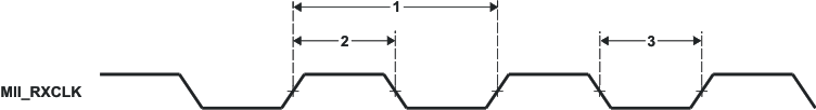 Figure 6-42 MII_RXCLK Timing (EMAC - Receive)
Table 6-79 Timing Requirements for MII_TXCLK (see Figure 6-43)
| NO. | 1.2V, 1.1V | 1.0V | UNIT | ||||||
|---|---|---|---|---|---|---|---|---|---|
| 10 Mbps | 100 Mbps | 10 Mbps | |||||||
| MIN | MAX | MIN | MAX | MIN | MAX | ||||
| 1 | tc(MII_TXCLK) | Cycle time, MII_TXCLK | 400 | 40 | 400 | ns | |||
| 2 | tw(MII_TXCLKH) | Pulse duration, MII_TXCLK high | 140 | 14 | 140 | ns | |||
| 3 | tw(MII_TXCLKL) | Pulse duration, MII_TXCLK low | 140 | 14 | 140 | ns | |||
 Figure 6-43 MII_TXCLK Timing (EMAC - Transmit)
Table 6-80 Timing Requirements for EMAC MII Receive 10/100 Mbit/s(1) (see Figure 6-44)
| NO. | 1.2V, 1.1V, 1.0V | UNIT | |||
|---|---|---|---|---|---|
| MIN | MAX | ||||
| 1 | tsu(MRXD-MII_RXCLKH) | Setup time, receive selected signals valid before MII_RXCLK high | 8 | ns | |
| 2 | th(MII_RXCLKH-MRXD) | Hold time, receive selected signals valid after MII_RXCLK high | 8 | ns | |
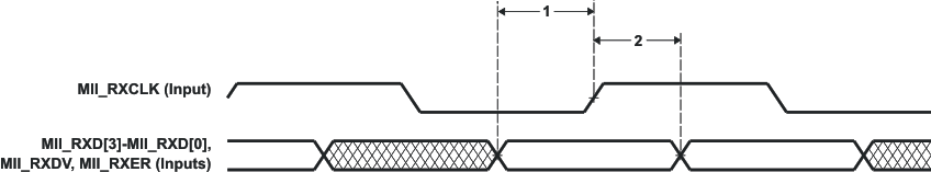 Figure 6-44 EMAC Receive Interface Timing
Table 6-81 Switching Characteristics Over Recommended Operating Conditions for EMAC MII Transmit 10/100 Mbit/s(1) (see Figure 6-45)
| NO. | PARAMETER | 1.2V, 1.1V | 1.0V | UNIT | |||
|---|---|---|---|---|---|---|---|
| MIN | MAX | MIN | MAX | ||||
| 1 | td(MII_TXCLKH-MTXD) | Delay time, MII_TXCLK high to transmit selected signals valid | 2 | 25 | 2 | 32 | ns |
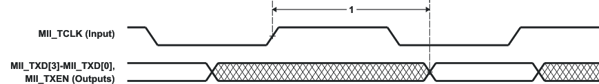 Figure 6-45 EMAC Transmit Interface Timing
Table 6-82 Timing Requirements for EMAC RMII
| NO. | 1.2V, 1.1V(1) | UNIT | ||||
|---|---|---|---|---|---|---|
| MIN | TYP | MAX | ||||
| 1 | tc(REFCLK) | Cycle Time, RMII_MHZ_50_CLK(2) | 20 | ns | ||
| 2 | tw(REFCLKH) | Pulse Width, RMII_MHZ_50_CLK High | 7 | 13 | ns | |
| 3 | tw(REFCLKL) | Pulse Width, RMII_MHZ_50_CLK Low | 7 | 13 | ns | |
| 6 | tsu(RXD-REFCLK) | Input Setup Time, RXD Valid before RMII_MHZ_50_CLK High | 4 | ns | ||
| 7 | th(REFCLK-RXD) | Input Hold Time, RXD Valid after RMII_MHZ_50_CLK High | 2 | ns | ||
| 8 | tsu(CRSDV-REFCLK) | Input Setup Time, CRSDV Valid before RMII_MHZ_50_CLK High | 4 | ns | ||
| 9 | th(REFCLK-CRSDV) | Input Hold Time, CRSDV Valid after RMII_MHZ_50_CLK High | 2 | ns | ||
| 10 | tsu(RXER-REFCLK) | Input Setup Time, RXER Valid before RMII_MHZ_50_CLK High | 4 | ns | ||
| 11 | th(REFCLKR-RXER) | Input Hold Time, RXER Valid after RMII_MHZ_50_CLK High | 2 | ns | ||
Table 6-83 Switching Characteristics Over Recommended Operating Conditions for EMAC RMII
| NO. | PARAMETER | 1.2V, 1.1V(1) | UNIT | |||
|---|---|---|---|---|---|---|
| MIN | TYP | MAX | ||||
| 4 | td(REFCLK-TXD) | Output Delay Time, RMII_MHZ_50_CLK High to TXD Valid | 2.5 | 13 | ns | |
| 5 | td(REFCLK-TXEN) | Output Delay Time, RMII_MHZ_50_CLK High to TXEN Valid | 2.5 | 13 | ns | |
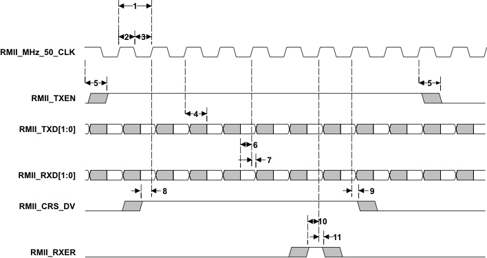 Figure 6-46 RMII Timing Diagram
6.20 Management Data Input/Output (MDIO)
The Management Data Input/Output (MDIO) module continuously polls all 32 MDIO addresses in order to enumerate all PHY devices in the system.
The Management Data Input/Output (MDIO) module implements the 802.3 serial management interface to interrogate and control Ethernet PHY(s) using a shared two-wire bus. Host software uses the MDIO module to configure the auto-negotiation parameters of each PHY attached to the EMAC, retrieve the negotiation results, and configure required parameters in the EMAC module for correct operation. The module is designed to allow almost transparent operation of the MDIO interface, with very little maintenance from the core processor. Only one PHY may be connected at any given time.
6.20.1 MDIO Registers
For a list of supported MDIO registers see Table 6-84 [MDIO Registers].
Table 6-84 MDIO Register Memory Map
| BYTE ADDRESS | ACRONYM | REGISTER NAME |
|---|---|---|
| 0x01E2 4000 | REV | Revision Identification Register |
| 0x01E2 4004 | CONTROL | MDIO Control Register |
| 0x01E2 4008 | ALIVE | MDIO PHY Alive Status Register |
| 0x01E2 400C | LINK | MDIO PHY Link Status Register |
| 0x01E2 4010 | LINKINTRAW | MDIO Link Status Change Interrupt (Unmasked) Register |
| 0x01E2 4014 | LINKINTMASKED | MDIO Link Status Change Interrupt (Masked) Register |
| 0x01E2 4018 | - | Reserved |
| 0x01E2 4020 | USERINTRAW | MDIO User Command Complete Interrupt (Unmasked) Register |
| 0x01E2 4024 | USERINTMASKED | MDIO User Command Complete Interrupt (Masked) Register |
| 0x01E2 4028 | USERINTMASKSET | MDIO User Command Complete Interrupt Mask Set Register |
| 0x01E2 402C | USERINTMASKCLEAR | MDIO User Command Complete Interrupt Mask Clear Register |
| 0x01E2 4030 - 0x01E2 407C | - | Reserved |
| 0x01E2 4080 | USERACCESS0 | MDIO User Access Register 0 |
| 0x01E2 4084 | USERPHYSEL0 | MDIO User PHY Select Register 0 |
| 0x01E2 4088 | USERACCESS1 | MDIO User Access Register 1 |
| 0x01E2 408C | USERPHYSEL1 | MDIO User PHY Select Register 1 |
| 0x01E2 4090 - 0x01E2 47FF | - | Reserved |
6.20.2 Management Data Input/Output (MDIO) Electrical Data/Timing
Table 6-85 Timing Requirements for MDIO Input (see Figure 6-47 and Figure 6-48)
| NO. | 1.3V, 1.2V, 1.1V | 1.0V | UNIT | ||||
|---|---|---|---|---|---|---|---|
| MIN | MAX | MIN | MAX | ||||
| 1 | tc(MDCLK) | Cycle time, MDCLK | 400 | 400 | ns | ||
| 2 | tw(MDCLK) | Pulse duration, MDCLK high/low | 180 | 180 | ns | ||
| 3 | tt(MDCLK) | Transition time, MDCLK | 5 | 5 | ns | ||
| 4 | tsu(MDIO-MDCLKH) | Setup time, MDIO data input valid before MDCLK high | 16 | 21 | ns | ||
| 5 | th(MDCLKH-MDIO) | Hold time, MDIO data input valid after MDCLK high | 0 | 0 | ns | ||
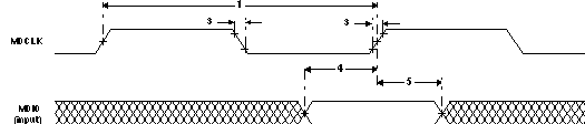 Figure 6-47 MDIO Input Timing
Table 6-86 Switching Characteristics Over Recommended Operating Conditions for MDIO Output
(see Figure 6-48)
| NO. | 1.1V, 1.0V | UNIT | |||
|---|---|---|---|---|---|
| MIN | MAX | ||||
| 7 | td(MDCLKL-MDIO) | Delay time, MDCLK low to MDIO data output valid | 0 | 100 | ns |
 Figure 6-48 MDIO Output Timing
6.21 Timers
The timers support the following features:
- Configurable as single 64-bit timer or two 32-bit timers
- Period timeouts generate interrupts, DMA events or external pin events
- 8 32-bit compare registers
- Compare matches generate interrupt events
- Capture capability
- 64-bit Watchdog capability (Timer64P1 only)
Table 6-87 Timer Registers
| TIMER64P 0 BYTE ADDRESS | TIMER64P 1 BYTE ADDRESS | TIMER64P 2 BYTE ADDRESS | TIMER64P 3 BYTE ADDRESS | ACRONYM | REGISTER DESCRIPTION |
|---|---|---|---|---|---|
| 0x01C2 0000 | 0x01C2 1000 | 0x01F0 C000 | 0x01F0 D000 | REV | Revision Register |
| 0x01C2 0004 | 0x01C2 1004 | 0x01F0 C004 | 0x01F0 D004 | EMUMGT | Emulation Management Register |
| 0x01C2 0008 | 0x01C2 1008 | 0x01F0 C008 | 0x01F0 D008 | GPINTGPEN | GPIO Interrupt and GPIO Enable Register |
| 0x01C2 000C | 0x01C2 100C | 0x01F0 C00C | 0x01F0 D00C | GPDATGPDIR | GPIO Data and GPIO Direction Register |
| 0x01C2 0010 | 0x01C2 1010 | 0x01F0 C010 | 0x01F0 D010 | TIM12 | Timer Counter Register 12 |
| 0x01C2 0014 | 0x01C2 1014 | 0x01F0 C014 | 0x01F0 D014 | TIM34 | Timer Counter Register 34 |
| 0x01C2 0018 | 0x01C2 1018 | 0x01F0 C018 | 0x01F0 D018 | PRD12 | Timer Period Register 12 |
| 0x01C2 001C | 0x01C2 101C | 0x01F0 C01C | 0x01F0 D01C | PRD34 | Timer Period Register 34 |
| 0x01C2 0020 | 0x01C2 1020 | 0x01F0 C020 | 0x01F0 D020 | TCR | Timer Control Register |
| 0x01C2 0024 | 0x01C2 1024 | 0x01F0 C024 | 0x01F0 D024 | TGCR | Timer Global Control Register |
| 0x01C2 0028 | 0x01C2 1028 | 0x01F0 C028 | 0x01F0 D028 | WDTCR | Watchdog Timer Control Register |
| 0x01C2 0034 | 0x01C2 1034 | 0x01F0 C034 | 0x01F0 D034 | REL12 | Timer Reload Register 12 |
| 0x01C2 0038 | 0x01C2 1038 | 0x01F0 C038 | 0x01F0 D038 | REL34 | Timer Reload Register 34 |
| 0x01C2 003C | 0x01C2 103C | 0x01F0 C03C | 0x01F0 D03C | CAP12 | Timer Capture Register 12 |
| 0x01C2 0040 | 0x01C2 1040 | 0x01F0 C040 | 0x01F0 D040 | CAP34 | Timer Capture Register 34 |
| 0x01C2 0044 | 0x01C2 1044 | 0x01F0 C044 | 0x01F0 D044 | INTCTLSTAT | Timer Interrupt Control and Status Register |
| 0x01C2 0060 | 0x01C2 1060 | 0x01F0 C060 | 0x01F0 D060 | CMP0 | Compare Register 0 |
| 0x01C2 0064 | 0x01C2 1064 | 0x01F0 C064 | 0x01F0 D064 | CMP1 | Compare Register 1 |
| 0x01C2 0068 | 0x01C2 1068 | 0x01F0 C068 | 0x01F0 D068 | CMP2 | Compare Register 2 |
| 0x01C2 006C | 0x01C2 106C | 0x01F0 C06C | 0x01F0 D06C | CMP3 | Compare Register 3 |
| 0x01C2 0070 | 0x01C2 1070 | 0x01F0 C070 | 0x01F0 D070 | CMP4 | Compare Register 4 |
| 0x01C2 0074 | 0x01C2 1074 | 0x01F0 C074 | 0x01F0 D074 | CMP5 | Compare Register 5 |
| 0x01C2 0078 | 0x01C2 1078 | 0x01F0 C078 | 0x01F0 D078 | CMP6 | Compare Register 6 |
| 0x01C2 007C | 0x01C2 107C | 0x01F0 C07C | 0x01F0 D07C | CMP7 | Compare Register 7 |
6.21.1 Timer Electrical Data/Timing
Table 6-88 Timing Requirements for Timer Input(1)(2) (see Figure 6-49)
| NO. | 1.2V, 1.1V, 1.0V | UNIT | |||
|---|---|---|---|---|---|
| MIN | MAX | ||||
| 1 | tc(TM64Px_IN12) | Cycle time, TM64Px_IN12 | 4P | ns | |
| 2 | tw(TINPH) | Pulse duration, TM64Px_IN12 high | 0.45C | 0.55C | ns |
| 3 | tw(TINPL) | Pulse duration, TM64Px_IN12 low | 0.45C | 0.55C | ns |
| 4 | tt(TM64Px_IN12) | Transition time, TM64Px_IN12 | 0.05C or 10(3) | ns | |
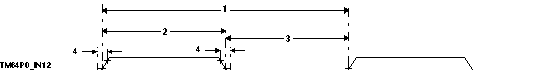 Figure 6-49 Timer Timing
Table 6-89 Switching Characteristics Over Recommended Operating Conditions for Timer Output (1)
| NO. | PARAMETER | 1.2V, 1.1V, 1.0V | UNIT | ||
|---|---|---|---|---|---|
| MIN | MAX | ||||
| 5 | tw(TOUTH) | Pulse duration, TM64P0_OUT12 high | 4P | ns | |
| 6 | tw(TOUTL) | Pulse duration, TM64P0_OUT12 low | 4P | ns | |
 Figure 6-50 Timer Timing
6.22 Real Time Clock (RTC)
The RTC provides a time reference to an application running on the device. The current date and time is tracked in a set of counter registers that update once per second. The time can be represented in 12-hour or 24-hour mode. The calendar and time registers are buffered during reads and writes so that updates do not interfere with the accuracy of the time and date.
Alarms are available to interrupt the CPU at a particular time, or at periodic time intervals, such as once per minute or once per day. In addition, the RTC can interrupt the CPU every time the calendar and time registers are updated, or at programmable periodic intervals.
The real-time clock (RTC) provides the following features:
- 100-year calendar (xx00 to xx99)
- Counts seconds, minutes, hours, day of the week, date, month, and year with leap year compensation
- Binary-coded-decimal (BCD) representation of time, calendar, and alarm
- 12-hour clock mode (with AM and PM) or 24-hour clock mode
- Alarm interrupt
- Periodic interrupt
- Single interrupt to the CPU
- Supports external 32.768-kHz crystal or external clock source of the same frequency
- Separate isolated power supply
Figure 6-51 shows a block diagram of the RTC.
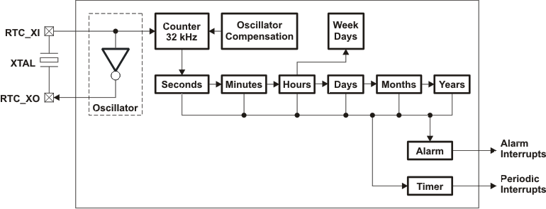 Figure 6-51 Real-Time Clock Block Diagram
6.22.1 Clock Source
The clock reference for the RTC is an external 32.768-kHz crystal or an external clock source of the same frequency. The RTC also has a separate power supply that is isolated from the rest of the system. When the CPU and other peripherals are without power, the RTC can remain powered to preserve the current time and calendar information. Even if the RTC is not used, it must remain powered when the rest of the device is powered.
The source for the RTC reference clock may be provided by a crystal or by an external clock source. The RTC has an internal oscillator buffer to support direct operation with a crystal. The crystal is connected between pins RTC_XI and RTC_XO. RTC_XI is the input to the on-chip oscillator and RTC_XO is the output from the oscillator back to the crystal.
An external 32.768-kHz clock source may be used instead of a crystal. In such a case, the clock source is connected to RTC_XI, and RTC_XO is left unconnected.
If the RTC is not used, the RTC_XI pin should be held either low or high, RTC_XO should be left unconnected, RTC_CVDD should be connected to the device CVDD and RTC_VSS should remain grounded.
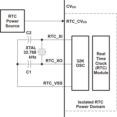 Figure 6-52 Clock Source
6.22.2 Real-Time Clock Register Descriptions
Table 6-90 Real-Time Clock (RTC) Registers
| BYTE ADDRESS | ACRONYM | REGISTER DESCRIPTION |
|---|---|---|
| 0x01C2 3000 | SECOND | Seconds Register |
| 0x01C2 3004 | MINUTE | Minutes Register |
| 0x01C2 3008 | HOUR | Hours Register |
| 0x01C2 300C | DAY | Day of the Month Register |
| 0x01C2 3010 | MONTH | Month Register |
| 0x01C2 3014 | YEAR | Year Register |
| 0x01C2 3018 | DOTW | Day of the Week Register |
| 0x01C2 3020 | ALARMSECOND | Alarm Seconds Register |
| 0x01C2 3024 | ALARMMINUTE | Alarm Minutes Register |
| 0x01C2 3028 | ALARMHOUR | Alarm Hours Register |
| 0x01C2 302C | ALARMDAY | Alarm Days Register |
| 0x01C2 3030 | ALARMMONTH | Alarm Months Register |
| 0x01C2 3034 | ALARMYEAR | Alarm Years Register |
| 0x01C2 3040 | CTRL | Control Register |
| 0x01C2 3044 | STATUS | Status Register |
| 0x01C2 3048 | INTERRUPT | Interrupt Enable Register |
| 0x01C2 304C | COMPLSB | Compensation (LSB) Register |
| 0x01C2 3050 | COMPMSB | Compensation (MSB) Register |
| 0x01C2 3054 | OSC | Oscillator Register |
| 0x01C2 3060 | SCRATCH0 | Scratch 0 (General-Purpose) Register |
| 0x01C2 3064 | SCRATCH1 | Scratch 1 (General-Purpose) Register |
| 0x01C2 3068 | SCRATCH2 | Scratch 2 (General-Purpose) Register |
| 0x01C2 306C | KICK0 | Kick 0 (Write Protect) Register |
| 0x01C2 3070 | KICK1 | Kick 1 (Write Protect) Register |
6.23 General-Purpose Input/Output (GPIO)
The GPIO peripheral provides general-purpose pins that can be configured as either inputs or outputs. When configured as an output, a write to an internal register can control the state driven on the output pin. When configured as an input, the state of the input is detectable by reading the state of an internal register. In addition, the GPIO peripheral can produce CPU interrupts and EDMA events in different interrupt/event generation modes. The GPIO peripheral provides generic connections to external devices. The GPIO pins are grouped into banks of 16 pins per bank (i.e., bank 0 consists of GPIO [0:15]).
The device GPIO peripheral supports the following:
- Up to 144 Pins configurable as GPIO
- External Interrupt and DMA request Capability
- Every GPIO pin may be configured to generate an interrupt request on detection of rising and/or falling edges on the pin.
- The interrupt requests within each bank are combined (logical or) to create eight unique bank level interrupt requests.
- The bank level interrupt service routine may poll the INTSTATx register for its bank to determine which pin(s) have triggered the interrupt.
- GPIO Banks 0, 1, 2, 3, 4, 5, 6, 7 and 8 Interrupts assigned to ARM INTC Interrupt Requests 42, 43, 44, 45, 46, 47, 48, 49 and 50 respectively
- GPIO Banks 0, 1, 2, 3, 4, and 5 are assigned to EDMA events 6, 7, 22, 23, 28, 29, and 29 respectively on Channel Controller 0 and GPIO Banks 6, 7, and 8 are assigned to EDMA events 16, 17, and 18 respectively on Channel Controller 1.
- Set/clear functionality: Firmware writes 1 to corresponding bit position(s) to set or to clear GPIO signal(s). This allows multiple firmware processes to toggle GPIO output signals without critical section protection (disable interrupts, program GPIO, re-enable interrupts, to prevent context switching to anther process during GPIO programming).
- Separate Input/Output registers
- Output register in addition to set/clear so that, if preferred by firmware, some GPIO output signals can be toggled by direct write to the output register(s).
- Output register, when read, reflects output drive status. This, in addition to the input register reflecting pin status and open-drain I/O cell, allows wired logic be implemented.
The memory map for the GPIO registers is shown in Table 6-91.
6.23.1 GPIO Register Description(s)
Table 6-91 GPIO Registers
| BYTE ADDRESS | ACRONYM | REGISTER DESCRIPTION |
|---|---|---|
| 0x01E2 6000 | REV | Peripheral Revision Register |
| 0x01E2 6004 | RESERVED | Reserved |
| 0x01E2 6008 | BINTEN | GPIO Interrupt Per-Bank Enable Register |
| GPIO Banks 0 and 1 | ||
| 0x01E2 6010 | DIR01 | GPIO Banks 0 and 1 Direction Register |
| 0x01E2 6014 | OUT_DATA01 | GPIO Banks 0 and 1 Output Data Register |
| 0x01E2 6018 | SET_DATA01 | GPIO Banks 0 and 1 Set Data Register |
| 0x01E2 601C | CLR_DATA01 | GPIO Banks 0 and 1 Clear Data Register |
| 0x01E2 6020 | IN_DATA01 | GPIO Banks 0 and 1 Input Data Register |
| 0x01E2 6024 | SET_RIS_TRIG01 | GPIO Banks 0 and 1 Set Rising Edge Interrupt Register |
| 0x01E2 6028 | CLR_RIS_TRIG01 | GPIO Banks 0 and 1 Clear Rising Edge Interrupt Register |
| 0x01E2 602C | SET_FAL_TRIG01 | GPIO Banks 0 and 1 Set Falling Edge Interrupt Register |
| 0x01E2 6030 | CLR_FAL_TRIG01 | GPIO Banks 0 and 1 Clear Falling Edge Interrupt Register |
| 0x01E2 6034 | INTSTAT01 | GPIO Banks 0 and 1 Interrupt Status Register |
| GPIO Banks 2 and 3 | ||
| 0x01E2 6038 | DIR23 | GPIO Banks 2 and 3 Direction Register |
| 0x01E2 603C | OUT_DATA23 | GPIO Banks 2 and 3 Output Data Register |
| 0x01E2 6040 | SET_DATA23 | GPIO Banks 2 and 3 Set Data Register |
| 0x01E2 6044 | CLR_DATA23 | GPIO Banks 2 and 3 Clear Data Register |
| 0x01E2 6048 | IN_DATA23 | GPIO Banks 2 and 3 Input Data Register |
| 0x01E2 604C | SET_RIS_TRIG23 | GPIO Banks 2 and 3 Set Rising Edge Interrupt Register |
| 0x01E2 6050 | CLR_RIS_TRIG23 | GPIO Banks 2 and 3 Clear Rising Edge Interrupt Register |
| 0x01E2 6054 | SET_FAL_TRIG23 | GPIO Banks 2 and 3 Set Falling Edge Interrupt Register |
| 0x01E2 6058 | CLR_FAL_TRIG23 | GPIO Banks 2 and 3 Clear Falling Edge Interrupt Register |
| 0x01E2 605C | INTSTAT23 | GPIO Banks 2 and 3 Interrupt Status Register |
| GPIO Banks 4 and 5 | ||
| 0x01E2 6060 | DIR45 | GPIO Banks 4 and 5 Direction Register |
| 0x01E2 6064 | OUT_DATA45 | GPIO Banks 4 and 5 Output Data Register |
| 0x01E2 6068 | SET_DATA45 | GPIO Banks 4 and 5 Set Data Register |
| 0x01E2 606C | CLR_DATA45 | GPIO Banks 4 and 5 Clear Data Register |
| 0x01E2 6070 | IN_DATA45 | GPIO Banks 4 and 5 Input Data Register |
| 0x01E2 6074 | SET_RIS_TRIG45 | GPIO Banks 4 and 5 Set Rising Edge Interrupt Register |
| 0x01E2 6078 | CLR_RIS_TRIG45 | GPIO Banks 4 and 5 Clear Rising Edge Interrupt Register |
| 0x01E2 607C | SET_FAL_TRIG45 | GPIO Banks 4 and 5 Set Falling Edge Interrupt Register |
| 0x01E2 6080 | CLR_FAL_TRIG45 | GPIO Banks 4 and 5 Clear Falling Edge Interrupt Register |
| 0x01E2 6084 | INTSTAT45 | GPIO Banks 4 and 5 Interrupt Status Register |
| GPIO Banks 6 and 7 | ||
| 0x01E2 6088 | DIR67 | GPIO Banks 6 and 7 Direction Register |
| 0x01E2 608C | OUT_DATA67 | GPIO Banks 6 and 7 Output Data Register |
| 0x01E2 6090 | SET_DATA67 | GPIO Banks 6 and 7 Set Data Register |
| 0x01E2 6094 | CLR_DATA67 | GPIO Banks 6 and 7 Clear Data Register |
| 0x01E2 6098 | IN_DATA67 | GPIO Banks 6 and 7 Input Data Register |
| 0x01E2 609C | SET_RIS_TRIG67 | GPIO Banks 6 and 7 Set Rising Edge Interrupt Register |
| 0x01E2 60A0 | CLR_RIS_TRIG67 | GPIO Banks 6 and 7 Clear Rising Edge Interrupt Register |
| 0x01E2 60A4 | SET_FAL_TRIG67 | GPIO Banks 6 and 7 Set Falling Edge Interrupt Register |
| 0x01E2 60A8 | CLR_FAL_TRIG67 | GPIO Banks 6 and 7 Clear Falling Edge Interrupt Register |
| 0x01E2 60AC | INTSTAT67 | GPIO Banks 6 and 7 Interrupt Status Register |
| GPIO Bank 8 | ||
| 0x01E2 60B0 | DIR8 | GPIO Bank 8 Direction Register |
| 0x01E2 60B4 | OUT_DATA8 | GPIO Bank 8 Output Data Register |
| 0x01E2 60B8 | SET_DATA8 | GPIO Bank 8 Set Data Register |
| 0x01E2 60BC | CLR_DATA8 | GPIO Bank 8 Clear Data Register |
| 0x01E2 60C0 | IN_DATA8 | GPIO Bank 8 Input Data Register |
| 0x01E2 60C4 | SET_RIS_TRIG8 | GPIO Bank 8 Set Rising Edge Interrupt Register |
| 0x01E2 60C8 | CLR_RIS_TRIG8 | GPIO Bank 8 Clear Rising Edge Interrupt Register |
| 0x01E2 60CC | SET_FAL_TRIG8 | GPIO Bank 8 Set Falling Edge Interrupt Register |
| 0x01E2 60D0 | CLR_FAL_TRIG8 | GPIO Bank 8 Clear Falling Edge Interrupt Register |
| 0x01E2 60D4 | INTSTAT8 | GPIO Bank 8 Interrupt Status Register |
6.23.2 GPIO Peripheral Input/Output Electrical Data/Timing
Table 6-92 Timing Requirements for GPIO Inputs(1) (see Figure 6-53)
| NO. | 1.2V, 1.1V, 1.0V | UNIT | |||
|---|---|---|---|---|---|
| MIN | MAX | ||||
| 1 | tw(GPIH) | Pulse duration, GPn[m] as input high | 2C(1)(2) | ns | |
| 2 | tw(GPIL) | Pulse duration, GPn[m] as input low | 2C(1)(2) | ns | |
Table 6-93 Switching Characteristics Over Recommended Operating Conditions for GPIO Outputs
(see Figure 6-53)
| NO. | PARAMETER | 1.2V, 1.1V, 1.0V | UNIT | ||
|---|---|---|---|---|---|
| MIN | MAX | ||||
| 3 | tw(GPOH) | Pulse duration, GPn[m] as output high | 2C(1)(2) | ns | |
| 4 | tw(GPOL) | Pulse duration, GPn[m] as output low | 2C(1)(2) | ns | |
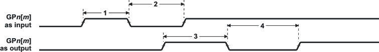 Figure 6-53 GPIO Port Timing
6.23.3 GPIO Peripheral External Interrupts Electrical Data/Timing
Table 6-94 Timing Requirements for External Interrupts(1) (see Figure 6-54)
| NO. | 1.2V, 1.1V, 1.0V | UNIT | ||||
|---|---|---|---|---|---|---|
| MIN | MAX | |||||
| 1 | tw(ILOW) | Width of the external interrupt pulse low | 2C(1)(2) | ns | ||
| 2 | tw(IHIGH) | Width of the external interrupt pulse high | 2C(1)(2) | ns | ||
 Figure 6-54 GPIO External Interrupt Timing
6.24 Emulation Logic
This section describes the steps to use a third party debugger on the ARM926EJ-S within the device. The debug capabilities and features for ARM are as shown below.
ARM:
- Basic Debug
- Execution Control
- System Visibility
- Advanced Debug
- Global Start
- Global Stop
- Advanced System Control
- Subsystem reset via debug
- Peripheral notification of debug events
- Cache-coherent debug accesses
- Program Trace
- Program flow corruption
- Code coverage
- Path coverage
- Thread/interrupt synchronization problems
- Data Trace
- Memory corruption
- Timing Trace
- Profiling
- Analysis Actions
- Stop program execution
- Control trace streams
- Generate debug interrupt
- Benchmarking with counters
- External trigger generation
- Debug state machine state transition
- Combinational and Sequential event generation
- Analysis Events
- Program event detection
- Data event detection
- External trigger Detection
- System event detection (i.e. cache miss)
- Debug state machine state detection
- Analysis Configuration
- Application access
- Debugger access
Table 6-95 ARM Debug Features
| Category | Hardware Feature | Availability |
|---|---|---|
| Basic Debug | Software breakpoint | Unlimited |
| Hardware breakpoint | Up to 14 HWBPs, including: | |
| 2 precise(1) HWBP inside ARM core which are shared with watch points. | ||
| 8 imprecise(1) HWBPs from ETM’s address comparators, which are shared with trace function, and can be used as watch points. | ||
| 4 imprecise(1) HWBPs from ICECrusher. | ||
| Analysis | Watch point | Up to 6 watch points, including: |
| 2 from ARM core which is shared with HWBPs and can be associated with a data. | ||
| 8 from ETM’s address comparators, which are shared with trace function, and HWBPs. | ||
| Watch point with Data | 2 from ARM core which is shared with HWBPs. | |
| 8 watch points from ETM can be associated with a data comparator, and ETM has total 4 data comparators. | ||
| Counters/timers | 3x32-bit (1 cycle ; 2 event) | |
| External Event Trigger In | 1 | |
| External Event Trigger Out | 1 | |
| Trace Control | Address range for trace | 4 |
| Data qualification for trace | 2 | |
| System events for trace control | 20 | |
| Counters/Timers for trace control | 2x16-bit | |
| State Machines/Sequencers | 1x3-State State Machine | |
| Context/Thread ID Comparator | 1 | |
| Independent trigger control units | 12 | |
| On-chip Trace Capture | Capture depth PC | 4k bytes ETB |
| Capture depth PC + Timing | 4k bytes ETB | |
| Application accessible | Y |
6.24.1 JTAG Port Description
The device target debug interface uses the five standard IEEE 1149.1(JTAG) signals (TRST, TCK, TMS, TDI, and TDO), a return clock (RTCK) due to the clocking requirements of the ARM926EJ-S and emulation signals EMU0 and EMU1. TRST holds the debug and boundary scan logic in reset when pulled low (its default state). Since TRST has an internal pull-down resistor, this ensures that at power up the device functions in its normal (non-test) operation mode if TRST is not connected. Otherwise, TRST should be driven inactive by the emulator or boundary scan controller. Boundary scan test cannot be performed while the TRST pin is pulled low.
Table 6-96 JTAG Port Description
| PIN | TYPE | NAME | DESCRIPTION |
|---|---|---|---|
| TRST | I | Test Logic Reset | When asserted (active low) causes all test and debug logic in the device to be reset along with the IEEE 1149.1 interface |
| TCK | I | Test Clock | This is the test clock used to drive an IEEE 1149.1 TAP state machine and logic. Depending on the emulator attached to , this is a free running clock or a gated clock depending on RTCK monitoring. |
| RTCK | O | Returned Test Clock | Synchronized TCK. Depending on the emulator attached to, the JTAG signals are clocked from RTCK or RTCK is monitored by the emulator to gate TCK. |
| TMS | I | Test Mode Select | Directs the next state of the IEEE 1149.1 test access port state machine |
| TDI | I | Test Data Input | Scan data input to the device |
| TDO | O | Test Data Output | Scan data output of the device |
| EMU0 | I/O | Emulation 0 | Channel 0 trigger + HSRTDX |
| EMU1 | I/O | Emulation 1 | Channel 1 trigger + HSRTDX |
6.24.2 Scan Chain Configuration Parameters
Table 6-97 shows the TAP configuration details required to configure the router/emulator for this device.
Table 6-97 JTAG Port Description
| Router Port ID | Default TAP | TAP Name | Tap IR Length |
|---|---|---|---|
| 17 | No | Reserved | 38 |
| 18 | No | ARM926 | 4 |
| 19 | No | ETB | 4 |
The router is revision C and has a 6-bit IR length.
6.24.3 Initial Scan Chain Configuration
The first level of debug interface that sees the scan controller is the TAP router module. The debugger can configure the TAP router for serially linking up to 16 TAP controllers or individually scanning one of the TAP controllers without disrupting the IR state of the other TAPs.
6.24.3.1 Adding TAPS to the Scan Chain
The TAP router must be programmed to add additional TAPs to the scan chain. The following JTAG scans must be completed to add the ARM926EJ-S to the scan chain.
A Power-On Reset (POR) or the JTAG Test-Logic Reset state configures the TAP router to contain only the router’s TAP.
 Figure 6-55 Adding ARM926EJ-S to the scan chain
Pre-amble: The device whose data reaches the emulator first is listed first in the board configuration file. This device is a pre-amble for all the other devices. This device has the lowest device ID.
Post-amble: The device whose data reaches the emulator last is listed last in the board configuration file. This device is a post-amble for all the other devices. This device has the highest device ID.
- Function : Update the JTAG preamble and post-amble counts.
- Parameter : The IR pre-amble count is '0'.
- Parameter : The IR post-amble count is '0'.
- Parameter : The DR pre-amble count is '0'.
- Parameter : The DR post-amble count is '0'.
- Parameter : The IR main count is '6'.
- Parameter : The DR main count is '1'.
- Function : Do a send-only JTAG IR/DR scan.
- Parameter : The route to JTAG shift state is 'shortest transition'.
- Parameter : The JTAG shift state is 'shift-ir'.
- Parameter : The JTAG destination state is 'pause-ir'.
- Parameter : The bit length of the command is '6'.
- Parameter : The send data value is '0x00000007'.
- Parameter : The actual receive data is 'discarded'.
- Function : Do a send-only JTAG IR/DR scan.
- Parameter : The route to JTAG shift state is 'shortest transition'.
- Parameter : The JTAG shift state is 'shift-dr'.
- Parameter : The JTAG destination state is 'pause-dr'.
- Parameter : The bit length of the command is '8'.
- Parameter : The send data value is '0x00000089'.
- Parameter : The actual receive data is 'discarded'.
- Function : Do a send-only JTAG IR/DR scan.
- Parameter : The route to JTAG shift state is 'shortest transition'.
- Parameter : The JTAG shift state is 'shift-ir'.
- Parameter : The JTAG destination state is 'pause-ir'.
- Parameter : The bit length of the command is '6'.
- Parameter : The send data value is '0x00000002'.
- Parameter : The actual receive data is 'discarded'.
- Function : Embed the port address in next command.
- Parameter : The port address field is '0x0f000000'.
- Parameter : The port address value is '3'.
- Function : Do a send-only JTAG IR/DR scan.
- Parameter : The route to JTAG shift state is 'shortest transition'.
- Parameter : The JTAG shift state is 'shift-dr'.
- Parameter : The JTAG destination state is 'pause-dr'.
- Parameter : The bit length of the command is '32'.
- Parameter : The send data value is '0xa2002108'.
- Parameter : The actual receive data is 'discarded'.
- Function : Do a send-only all-ones JTAG IR/DR scan.
- Parameter : The JTAG shift state is 'shift-ir'.
- Parameter : The JTAG destination state is 'run-test/idle'.
- Parameter : The bit length of the command is '6'.
- Parameter : The send data value is 'all-ones'.
- Parameter : The actual receive data is 'discarded'.
- Function : Wait for a minimum number of TCLK pulses.
- Parameter : The count of TCLK pulses is '10'.
- Function : Update the JTAG preamble and post-amble counts.
- Parameter : The IR pre-amble count is '0'.
- Parameter : The IR post-amble count is '6'.
- Parameter : The DR pre-amble count is '0'.
- Parameter : The DR post-amble count is '1'.
- Parameter : The IR main count is '4'.
- Parameter : The DR main count is '1'.
The initial scan chain contains only the TAP router module. The following steps must be completed in order to add ETB TAP to the scan chain.
 Figure 6-56 Adding ETB to the scan chain
- Function : Do a send-only JTAG IR/DR scan.
- Parameter : The route to JTAG shift state is 'shortest transition'.
- Parameter : The JTAG shift state is 'shift-ir'.
- Parameter : The JTAG destination state is 'pause-ir'.
- Parameter : The bit length of the command is '6'.
- Parameter : The send data value is '0x00000007'.
- Parameter : The actual receive data is 'discarded'.
- Function : Do a send-only JTAG IR/DR scan.
- Parameter : The route to JTAG shift state is 'shortest transition'.
- Parameter : The JTAG shift state is 'shift-dr'.
- Parameter : The JTAG destination state is 'pause-dr'.
- Parameter : The bit length of the command is '8'.
- Parameter : The send data value is '0x00000089'.
- Parameter : The actual receive data is 'discarded'.
- Function : Do a send-only JTAG IR/DR scan.
- Parameter : The route to JTAG shift state is 'shortest transition'.
- Parameter : The JTAG shift state is 'shift-ir'.
- Parameter : The JTAG destination state is 'pause-ir'.
- Parameter : The bit length of the command is '6'.
- Parameter : The send data value is '0x00000002'.
- Parameter : The actual receive data is 'discarded'.
- Function : Embed the port address in next command.
- Parameter : The port address field is '0x0f000000'.
- Parameter : The port address value is '3'.
- Function : Do a send-only JTAG IR/DR scan.
- Parameter : The route to JTAG shift state is 'shortest transition'.
- Parameter : The JTAG shift state is 'shift-dr'.
- Parameter : The JTAG destination state is 'pause-dr'.
- Parameter : The bit length of the command is '32'.
- Parameter : The send data value is '0xa3302108'.
- Parameter : The actual receive data is 'discarded'.
- Function : Do a send-only all-ones JTAG IR/DR scan.
- Parameter : The JTAG shift state is 'shift-ir'.
- Parameter : The JTAG destination state is 'run-test/idle'.
- Parameter : The bit length of the command is '6'.
- Parameter : The send data value is 'all-ones'.
- Parameter : The actual receive data is 'discarded'.
- Function : Wait for a minimum number of TCLK pulses.
- Parameter : The count of TCLK pulses is '10'.
- Function : Update the JTAG preamble and post-amble counts.
- Parameter : The IR pre-amble count is '0'.
- Parameter : The IR post-amble count is '6 + 4'.
- Parameter : The DR pre-amble count is '0'.
- Parameter : The DR post-amble count is '1 + 1'.
- Parameter : The IR main count is '4'.
- Parameter : The DR main count is '1'.
6.24.4 IEEE 1149.1 JTAG
The JTAG
The device requires that both TRST and RESET be asserted upon power up to be properly initialized. While RESET initializes the device, TRST initializes the device's emulation logic. Both resets are required for proper operation.
While both TRST and RESET need to be asserted upon power up, only RESET needs to be released for the device to boot properly. TRST may be asserted indefinitely for normal operation, keeping the JTAG port interface and device's emulation logic in the reset state.
TRST only needs to be released when it is necessary to use a JTAG controller to debug the device or exercise the device's boundary scan functionality. Note: TRST is synchronous and must be clocked by TCK; otherwise, the boundary scan logic may not respond as expected after TRST is asserted.
RESET must be released only in order for boundary-scan JTAG to read the variant field of IDCODE correctly. Other boundary-scan instructions work correctly independent of current state of RESET.
For maximum reliability, the device includes an internal pulldown (IPD) on the TRST pin to ensure that TRST will always be asserted upon power up and the device's internal emulation logic will always be properly initialized.
JTAG controllers from Texas Instruments actively drive TRST high. However, some third-party JTAG controllers may not drive TRST high but expect the use of a pullup resistor on TRST.
When using this type of JTAG controller, assert TRST to initialize the device after powerup and externally drive TRST high before attempting any emulation or boundary scan operations.
6.24.4.1 JTAG Peripheral Register Description(s) - JTAG ID Register (DEVIDR0)
Table 6-98 DEVIDR0 Register
| BYTE ADDRESS | ACRONYM | REGISTER DESCRIPTION | COMMENTS |
|---|---|---|---|
| 0x01C1 4018 | DEVIDR0 | JTAG Identification Register | Read-only. Provides 32-bit JTAG ID of the device. |
The JTAG ID register is a read-only register that identifies to the customer the JTAG/Device ID. For the device, the JTAG ID register resides at address location 0x01C1 4018. The register hex value for each silicon revision is
- 0x1B7D 102F for silicon revision 2.0
| 31-28 | 27-12 | 11-1 | 0 | ||||
| VARIANT (4-Bit) | PART NUMBER (16-Bit) | MANUFACTURER (11-Bit) | LSB | ||||
| R-xxxx | R-1011 0111 1101 0001 | R-0000 0010 111 | R-1 | ||||
| LEGEND: R = Read, W = Write, n = value at reset |
Table 6-99 JTAG ID Register Selection Bit Descriptions
| BIT | NAME | DESCRIPTION |
|---|---|---|
| 31:28 | VARIANT | Variant (4-Bit) value |
| 27:12 | PART NUMBER | Part Number (16-Bit) value |
| 11-1 | MANUFACTURER | Manufacturer (11-Bit) value |
| 0 | LSB | LSB. This bit is read as a "1". |
6.24.4.2 JTAG Test-Port Electrical Data/Timing
Table 6-100 Timing Requirements for JTAG Test Port (see Figure 6-58)
| No. | 1.2V | 1.1V | 1.0V | UNIT | |||||
|---|---|---|---|---|---|---|---|---|---|
| MIN | MAX | MIN | MAX | MIN | MAX | ||||
| 1 | tc(TCK) | Cycle time, TCK | 40 | 50 | 66.6 | ns | |||
| 2 | tw(TCKH) | Pulse duration, TCK high | 16 | 20 | 26.6 | ns | |||
| 3 | tw(TCKL) | Pulse duration, TCK low | 16 | 20 | 26.6 | ns | |||
| 4 | tc(RTCK) | Cycle time, RTCK | 40 | 50 | 66.6 | ns | |||
| 5 | tw(RTCKH) | Pulse duration, RTCK high | 16 | 20 | 26.6 | ns | |||
| 6 | tw(RTCKL) | Pulse duration, RTCK low | 16 | 20 | 26.6 | ns | |||
| 7 | tsu(TDIV-RTCKH) | Setup time, TDI/TMS/TRST valid before RTCK high | 4 | 4 | 4 | ns | |||
| 8 | th(RTCKH-TDIV) | Hold time, TDI/TMS/TRST valid after RTCK high | 4 | 6 | 8 | ns | |||
Table 6-101 Switching Characteristics Over Recommended Operating Conditions for JTAG Test Port
(see Figure 6-58)
| No. | PARAMETER | 1.2V | 1.1V | 1.0V | UNIT | ||||
|---|---|---|---|---|---|---|---|---|---|
| MIN | MAX | MIN | MAX | MIN | MAX | ||||
| 9 | td(RTCKL-TDOV) | Delay time, RTCK low to TDO valid | 18 | 23 | 31 | ns | |||
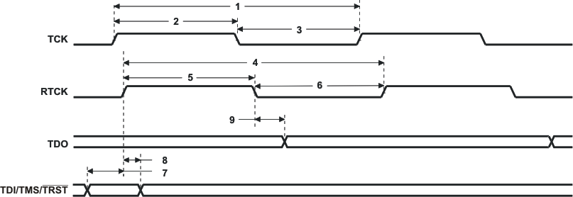 Figure 6-58 JTAG Test-Port Timing
6.24.5 JTAG 1149.1 Boundary Scan Considerations
To use boundary scan, the following sequence should be followed:
- Execute a valid reset sequence and exit reset
- Wait at least 6000 OSCIN clock cycles
- Enter boundary scan mode using the JTAG pins