SPRS709D November 2010 – March 2014 AM1810
PRODUCTION DATA.
- 1 AM1810 ARM Microprocessor For PROFIBUS
- 2Revision History
-
3Device Overview
- 3.1 Device Characteristics
- 3.2 Device Compatibility
- 3.3 ARM Subsystem
- 3.4 Memory Map Summary
- 3.5 Pin Assignments
- 3.6 Pin Multiplexing Control
- 3.7
Terminal Functions
- 3.7.1 Device Reset and JTAG
- 3.7.2 High-Frequency Oscillator and PLL
- 3.7.3 Real-Time Clock and 32-kHz Oscillator
- 3.7.4 DEEPSLEEP Power Control
- 3.7.5 External Memory Interface A (EMIFA)
- 3.7.6 DDR2/mDDR Memory Controller
- 3.7.7 Serial Peripheral Interface Modules (SPI)
- 3.7.8 PROFIBUS Real-Time Unit (PRU)
- 3.7.9 Enhanced Capture/Auxiliary PWM Modules (eCAP0)
- 3.7.10 Enhanced Pulse Width Modulators (eHRPWM)
- 3.7.11 Boot
- 3.7.12 Universal Asynchronous Receiver/Transmitters (UART0, UART1, UART2)
- 3.7.13 Inter-Integrated Circuit Modules(I2C0, I2C1)
- 3.7.14 Timers
- 3.7.15 Multichannel Audio Serial Ports (McASP)
- 3.7.16 Multichannel Buffered Serial Ports (McBSP)
- 3.7.17 Universal Serial Bus Modules (USB0, USB1)
- 3.7.18 Ethernet Media Access Controller (EMAC)
- 3.7.19 Multimedia Card/Secure Digital (MMC/SD)
- 3.7.20 Liquid Crystal Display Controller(LCD)
- 3.7.21 Serial ATA Controller (SATA)
- 3.7.22 Universal Host-Port Interface (UHPI)
- 3.7.23 Universal Parallel Port (uPP)
- 3.7.24 Video Port Interface (VPIF)
- 3.7.25 General Purpose Input Output
- 3.7.26 Reserved and No Connect
- 3.7.27 Supply and Ground
- 3.8 Unused Pin Configurations
- 4Device Configuration
-
5Specifications
- 5.1 Absolute Maximum Ratings Over Operating Junction Temperature Range (Unless Otherwise Noted)
- 5.2 Handling Ratings
- 5.3 Recommended Operating Conditions
- 5.4 Notes on Recommended Power-On Hours (POH)
- 5.5 Electrical Characteristics Over Recommended Ranges of Supply Voltage and Operating Junction Temperature (Unless Otherwise Noted)
-
6Peripheral Information and Electrical Specifications
- 6.1 Parameter Information
- 6.2 Recommended Clock and Control Signal Transition Behavior
- 6.3 Power Supplies
- 6.4 Reset
- 6.5 Crystal Oscillator or External Clock Input
- 6.6 Clock PLLs
- 6.7 Interrupts
- 6.8 Power and Sleep Controller (PSC)
- 6.9 EDMA
- 6.10 External Memory Interface A (EMIFA)
- 6.11
DDR2/mDDR Memory Controller
- 6.11.1 DDR2/mDDR Memory Controller Electrical Data/Timing
- 6.11.2 DDR2/mDDR Controller Register Description(s)
- 6.11.3
DDR2/mDDR Interface
- 6.11.3.1 DDR2/mDDR Interface Schematic
- 6.11.3.2 Compatible JEDEC DDR2/mDDR Devices
- 6.11.3.3 PCB Stackup
- 6.11.3.4 Placement
- 6.11.3.5 DDR2/mDDR Keep Out Region
- 6.11.3.6 Bulk Bypass Capacitors
- 6.11.3.7 High-Speed Bypass Capacitors
- 6.11.3.8 Net Classes
- 6.11.3.9 DDR2/mDDR Signal Termination
- 6.11.3.10 VREF Routing
- 6.11.3.11 DDR2/mDDR CK and ADDR_CTRL Routing
- 6.11.3.12 MDDR/DDR2 Boundary Scan Limitations
- 6.12 Memory Protection Units
- 6.13 MMC / SD / SDIO (MMCSD0, MMCSD1)
- 6.14 Serial ATA Controller (SATA)
- 6.15 Multichannel Audio Serial Port (McASP)
- 6.16 Multichannel Buffered Serial Port (McBSP)
- 6.17 Serial Peripheral Interface Ports (SPI0, SPI1)
- 6.18 Inter-Integrated Circuit Serial Ports (I2C)
- 6.19 Universal Asynchronous Receiver/Transmitter (UART)
- 6.20 Universal Serial Bus OTG Controller (USB0) [USB2.0 OTG]
- 6.21 Universal Serial Bus Host Controller (USB1) [USB1.1 OHCI]
- 6.22 Ethernet Media Access Controller (EMAC)
- 6.23 Management Data Input/Output (MDIO)
- 6.24 LCD Controller (LCDC)
- 6.25 Host-Port Interface (UHPI)
- 6.26 Universal Parallel Port (uPP)
- 6.27 Video Port Interface (VPIF)
- 6.28 Enhanced Capture (eCAP) Peripheral
- 6.29 Enhanced High-Resolution Pulse-Width Modulator (eHRPWM)
- 6.30 Timers
- 6.31 Real Time Clock (RTC)
- 6.32 General-Purpose Input/Output (GPIO)
- 6.33 Programmable Real-Time Unit Subsystem (PRUSS) With PROFIBUS
- 6.34 Emulation Logic
- 7Device and Documentation Support
- 8Mechanical Packaging and Orderable Information
Package Options
Refer to the PDF data sheet for device specific package drawings
Mechanical Data (Package|Pins)
- ZWT|361
Thermal pad, mechanical data (Package|Pins)
Orderable Information
3 Device Overview
3.1 Device Characteristics
Table 3-1 provides an overview of the device. The table shows significant features of the device, including the capacity of on-chip RAM, peripherals, and the package type with pin count.
Table 3-1 Characteristics of the Device
| HARDWARE FEATURES | AM1810 | |||
|---|---|---|---|---|
| Peripherals Not all peripherals pins are available at the same time (for more detail, see the Device Configurations section). |
DDR2/mDDR Controller | DDR2, 16-bit bus width, up to 156 MHz Mobile DDR, 16-bit bus width, up to 150 MHz |
||
| EMIFA | Asynchronous (8/16-bit bus width) RAM, Flash, 16-bit SDRAM, NOR, NAND |
|||
| Flash Card Interface | MMC and SD cards supported | |||
| EDMA3 | 64 independent channels, 16 QDMA channels, 2 channel controllers, 3 transfer controllers |
|||
| Timers | 4 64-Bit General Purpose (each configurable as 2 separate 32-bit timers, one configurable as Watch Dog) | |||
| UART | 3 (each with RTS and CTS flow control) | |||
| SPI | 2 (Each with one hardware chip select) | |||
| I2C | 2 (both Master/Slave) | |||
| Multichannel Audio Serial Port [McASP] | 1 (each with transmit/receive, FIFO buffer, 16 serializers) | |||
| Multichannel Buffered Serial Port [McBSP] | 2 (each with transmit/receive, FIFO buffer, 16) | |||
| 10/100 Ethernet MAC with Management Data I/O | 1 (MII or RMII Interface) | |||
| eHRPWM | 4 Single Edge, 4 Dual Edge Symmetric, or 2 Dual Edge Asymmetric Outputs |
|||
| eCAP | 3 32-bit capture inputs or 3 32-bit auxiliary PWM outputs | |||
| USB 2.0 (USB0) | High-Speed OTG Controller with on-chip OTG PHY | |||
| USB 1.1 (USB1) | Full-Speed OHCI (as host) with on-chip PHY | |||
| General-Purpose Input/Output Port | 9 banks of 16-bit | |||
| LCD Controller | 1 | |||
| SATA Controller | 1 (Supports both SATA I and SATAII) | |||
| Universal Parallel Port (uPP) | 1 | |||
| Video Port Interface (VPIF) | 1 (video in and video out) | |||
| PRU Subsystem (PRUSS) | 2 Programmable PRU Cores | |||
| On-Chip Memory | Size (Bytes) | 168KB RAM | ||
| Organization | ARM 16KB I-Cache 16KB D-Cache 8KB RAM (Vector Table) 64KB ROM ADDITIONAL MEMORY 128KB RAM |
|||
| JTAG BSDL_ID | DEVIDR0 Register | 0x0B7D_102F | ||
| CPU Frequency | MHz | ARM926 375 MHz (1.2V) | ||
| Voltage | Core (V) | 1.2 V nominal for 375 MHz version | ||
| I/O (V) | 1.8V or 3.3 V | |||
| Packages | 16 mm x 16 mm, 361-Ball 0.80 mm pitch, PBGA (ZWT) | |||
| Product Status(1) | Product Preview (PP), Advance Information (AI), or Production Data (PD) |
PD | ||
3.2 Device Compatibility
The ARM926EJ-S RISC CPU is compatible with other ARM9 CPUs from ARM Holdings plc.
3.3 ARM Subsystem
The ARM Subsystem includes the following features:
- ARM926EJ-S RISC processor
- ARMv5TEJ (32/16-bit) instruction set
- Little endian
- System Control Co-Processor 15 (CP15)
- MMU
- 16KB Instruction cache
- 16KB Data cache
- Write Buffer
- Embedded Trace Module and Embedded Trace Buffer (ETM/ETB)
- ARM Interrupt controller
3.3.1 ARM926EJ-S RISC CPU
The ARM Subsystem integrates the ARM926EJ-S processor. The ARM926EJ-S processor is a member of ARM9 family of general-purpose microprocessors. This processor is targeted at multi-tasking applications where full memory management, high performance, low die size, and low power are all important. The ARM926EJ-S processor supports the 32-bit ARM and 16 bit THUMB instruction sets, enabling the user to trade off between high performance and high code density. Specifically, the ARM926EJ-S processor supports the ARMv5TEJ instruction set, which includes features for efficient execution of Java byte codes, providing Java performance similar to Just in Time (JIT) Java interpreter, but without associated code overhead.
The ARM926EJ-S processor supports the ARM debug architecture and includes logic to assist in both hardware and software debug. The ARM926EJ-S processor has a Harvard architecture and provides a complete high performance subsystem, including:
- ARM926EJ -S integer core
- CP15 system control coprocessor
- Memory Management Unit (MMU)
- Separate instruction and data caches
- Write buffer
- Separate instruction and data (internal RAM) interfaces
- Separate instruction and data AHB bus interfaces
- Embedded Trace Module and Embedded Trace Buffer (ETM/ETB)
For more complete details on the ARM9, refer to the ARM926EJ-S Technical Reference Manual, available at http://www.arm.com
3.3.2 CP15
The ARM926EJ-S system control coprocessor (CP15) is used to configure and control instruction and data caches, Memory Management Unit (MMU), and other ARM subsystem functions. The CP15 registers are programmed using the MRC and MCR ARM instructions, when the ARM in a privileged mode such as supervisor or system mode.
3.3.3 MMU
A single set of two level page tables stored in main memory is used to control the address translation, permission checks and memory region attributes for both data and instruction accesses. The MMU uses a single unified Translation Lookaside Buffer (TLB) to cache the information held in the page tables. The MMU features are:
- Standard ARM architecture v4 and v5 MMU mapping sizes, domains and access protection scheme.
- Mapping sizes are:
- 1MB (sections)
- 64KB (large pages)
- 4KB (small pages)
- 1KB (tiny pages)
- Access permissions for large pages and small pages can be specified separately for each quarter of the page (subpage permissions)
- Hardware page table walks
- Invalidate entire TLB, using CP15 register 8
- Invalidate TLB entry, selected by MVA, using CP15 register 8
- Lockdown of TLB entries, using CP15 register 10
3.3.4 Caches and Write Buffer
The size of the Instruction cache is 16KB, Data cache is 16KB. Additionally, the caches have the following features:
- Virtual index, virtual tag, and addressed using the Modified Virtual Address (MVA)
- Four-way set associative, with a cache line length of eight words per line (32-bytes per line) and with two dirty bits in the Dcache
- Dcache supports write-through and write-back (or copy back) cache operation, selected by memory region using the C and B bits in the MMU translation tables
- Critical-word first cache refilling
- Cache lockdown registers enable control over which cache ways are used for allocation on a line fill, providing a mechanism for both lockdown, and controlling cache corruption
- Dcache stores the Physical Address TAG (PA TAG) corresponding to each Dcache entry in the TAG RAM for use during the cache line write-backs, in addition to the Virtual Address TAG stored in the TAG RAM. This means that the MMU is not involved in Dcache write-back operations, removing the possibility of TLB misses related to the write-back address.
- Cache maintenance operations provide efficient invalidation of, the entire Dcache or Icache, regions of the Dcache or Icache, and regions of virtual memory.
The write buffer is used for all writes to a noncachable bufferable region, write-through region and write misses to a write-back region. A separate buffer is incorporated in the Dcache for holding write-back for cache line evictions or cleaning of dirty cache lines. The main write buffer has 16-word data buffer and a four-address buffer. The Dcache write-back has eight data word entries and a single address entry.
3.3.5 Advanced High-Performance Bus (AHB)
The ARM Subsystem uses the AHB port of the ARM926EJ-S to connect the ARM to the Config bus and the external memories. Arbiters are employed to arbitrate access to the separate D-AHB and I-AHB by the Config Bus and the external memories bus.
3.3.6 Embedded Trace Macrocell (ETM) and Embedded Trace Buffer (ETB)
To support real-time trace, the ARM926EJ-S processor provides an interface to enable connection of an Embedded Trace Macrocell (ETM). The ARM926ES-J Subsystem in the device also includes the Embedded Trace Buffer (ETB). The ETM consists of two parts:
- Trace Port provides real-time trace capability for the ARM9.
- Triggering facilities provide trigger resources, which include address and data comparators, counter, and sequencers.
The device trace port is not pinned out and is instead only connected to the Embedded Trace Buffer. The ETB has a 4KB buffer memory. ETB enabled debug tools are required to read/interpret the captured trace data.
3.3.7 ARM Memory Mapping
By default the ARM has access to most on and off chip memory areas, including EMIFA, DDR2, and the additional 128K byte on chip SRAM. Likewise almost all of the on chip peripherals are accessible to the ARM by default.
To improve security and/or robustness, the device has extensive memory and peripheral protection units which can be configured to limit access rights to the various on/off chip resources to specific hosts; including the ARM as well as other master peripherals. This allows the system tasks to be partitioned between the ARM and DSP as best suites the particular application; while enhancing the overall robustness of the solution.
See Table 3-2 for a detailed top level device memory map that includes the ARM memory space.
3.4 Memory Map Summary
Note: Read/Write accesses to illegal or reserved addresses in the memory map may cause undefined behavior.
Table 3-2 Device Top Level Memory Map
| Start Address | End Address | Size | ARM Mem Map | EDMA Mem Map | PRUSS Mem Map | Master Peripheral Mem Map | LCDC Mem Map |
|---|---|---|---|---|---|---|---|
| 0x0000 0000 | 0x0000 0FFF | 4K | PRUSS Local Address Space | ||||
| 0x0000 1000 | 0x01BB FFFF | ||||||
| 0x01BC 0000 | 0x01BC 0FFF | 4K | ARM ETB memory | ||||
| 0x01BC 1000 | 0x01BC 17FF | 2K | ARM ETB reg | ||||
| 0x01BC 1800 | 0x01BC 18FF | 256 | ARM Ice Crusher | ||||
| 0x01BC 1900 | 0x01BF FFFF | ||||||
| 0x01C0 0000 | 0x01C0 7FFF | 32K | EDMA3 CC | ||||
| 0x01C0 8000 | 0x01C0 83FF | 1K | EDMA3 TC0 | ||||
| 0x01C0 8400 | 0x01C0 87FF | 1K | EDMA3 TC1 | ||||
| 0x01C0 8800 | 0x01C0 FFFF | ||||||
| 0x01C1 0000 | 0x01C1 0FFF | 4K | PSC 0 | ||||
| 0x01C1 1000 | 0x01C1 1FFF | 4K | PLL Controller 0 | ||||
| 0x01C1 2000 | 0x01C1 3FFF | ||||||
| 0x01C1 4000 | 0x01C1 4FFF | 4K | SYSCFG0 | ||||
| 0x01C1 5000 | 0x01C1 FFFF | ||||||
| 0x01C2 0000 | 0x01C2 0FFF | 4K | Timer0 | ||||
| 0x01C2 1000 | 0x01C2 1FFF | 4K | Timer1 | ||||
| 0x01C2 2000 | 0x01C2 2FFF | 4K | I2C 0 | ||||
| 0x01C2 3000 | 0x01C2 3FFF | 4K | RTC | ||||
| 0x01C2 4000 | 0x01C3 FFFF | ||||||
| 0x01C4 0000 | 0x01C4 0FFF | 4K | MMC/SD 0 | ||||
| 0x01C4 1000 | 0x01C4 1FFF | 4K | SPI 0 | ||||
| 0x01C4 2000 | 0x01C4 2FFF | 4K | UART 0 | ||||
| 0x01C4 3000 | 0x01CF FFFF | ||||||
| 0x01D0 0000 | 0x01D0 0FFF | 4K | McASP 0 Control | ||||
| 0x01D0 1000 | 0x01D0 1FFF | 4K | McASP 0 AFIFO Ctrl | ||||
| 0x01D0 2000 | 0x01D0 2FFF | 4K | McASP 0 Data | ||||
| 0x01D0 3000 | 0x01D0 BFFF | ||||||
| 0x01D0 C000 | 0x01D0 CFFF | 4K | UART 1 | ||||
| 0x01D0 D000 | 0x01D0 DFFF | 4K | UART 2 | ||||
| 0x01D0 E000 | 0x01D0 FFFF | ||||||
| 0x01D1 0000 | 0x01D1 07FF | 2K | McBSP0 | ||||
| 0x01D1 0800 | 0x01D1 0FFF | 2K | McBSP0 FIFO Ctrl | ||||
| 0x01D1 1000 | 0x01D1 17FF | 2K | McBSP1 | ||||
| 0x01D1 1800 | 0x01D1 1FFF | 2K | McBSP1 FIFO Ctrl | ||||
| 0x01D1 2000 | 0x01DF FFFF | ||||||
| 0x01E0 0000 | 0x01E0 FFFF | 64K | USB0 | ||||
| 0x01E1 0000 | 0x01E1 0FFF | 4K | UHPI | ||||
| 0x01E1 1000 | 0x01E1 2FFF | ||||||
| 0x01E1 3000 | 0x01E1 3FFF | 4K | LCD Controller | ||||
| 0x01E1 4000 | 0x01E1 4FFF | 4K | Memory Protection Unit 1 (MPU 1) | ||||
| 0x01E1 5000 | 0x01E1 5FFF | 4K | Memory Protection Unit 2 (MPU 2) | ||||
| 0x01E1 6000 | 0x01E1 6FFF | 4K | UPP | ||||
| 0x01E1 7000 | 0x01E1 7FFF | 4K | VPIF | ||||
| 0x01E1 8000 | 0x01E1 9FFF | 8K | SATA | ||||
| 0x01E1 A000 | 0x01E1 AFFF | 4K | PLL Controller 1 | ||||
| 0x01E1 B000 | 0x01E1 BFFF | 4K | MMCSD1 | ||||
| 0x01E1 C000 | 0x01E1 FFFF | ||||||
| 0x01E2 0000 | 0x01E2 1FFF | 8K | EMAC Control Module RAM | ||||
| 0x01E2 2000 | 0x01E2 2FFF | 4K | EMAC Control Module Registers | ||||
| 0x01E2 3000 | 0x01E2 3FFF | 4K | EMAC Control Registers | ||||
| 0x01E2 4000 | 0x01E2 4FFF | 4K | EMAC MDIO port | ||||
| 0x01E2 5000 | 0x01E2 5FFF | 4K | USB1 | ||||
| 0x01E2 6000 | 0x01E2 6FFF | 4K | GPIO | ||||
| 0x01E2 7000 | 0x01E2 7FFF | 4K | PSC 1 | ||||
| 0x01E2 8000 | 0x01E2 8FFF | 4K | I2C 1 | ||||
| 0x01E2 9000 | 0x01E2 BFFF | ||||||
| 0x01E2 C000 | 0x01E2 CFFF | 4K | SYSCFG1 | ||||
| 0x01E2 D000 | 0x01E2 FFFF | ||||||
| 0x01E3 0000 | 0x01E3 7FFF | 32K | EDMA3 CC1 | ||||
| 0x01E3 8000 | 0x01E3 83FF | 1K | EDMA3 TC2 | ||||
| 0x01E3 8400 | 0x01EF FFFF | ||||||
| 0x01F0 0000 | 0x01F0 0FFF | 4K | eHRPWM 0 | ||||
| 0x01F0 1000 | 0x01F0 1FFF | 4K | HRPWM 0 | ||||
| 0x01F0 2000 | 0x01F0 2FFF | 4K | eHRPWM 1 | ||||
| 0x01F0 3000 | 0x01F0 3FFF | 4K | HRPWM 1 | ||||
| 0x01F0 4000 | 0x01F0 5FFF | ||||||
| 0x01F0 6000 | 0x01F0 6FFF | 4K | ECAP 0 | ||||
| 0x01F0 7000 | 0x01F0 7FFF | 4K | ECAP 1 | ||||
| 0x01F0 8000 | 0x01F0 8FFF | 4K | ECAP 2 | ||||
| 0x01F0 9000 | 0x01F0 BFFF | ||||||
| 0x01F0 C000 | 0x01F0 CFFF | 4K | Timer2 | ||||
| 0x01F0 D000 | 0x01F0 DFFF | 4K | Timer3 | ||||
| 0x01F0 E000 | 0x01F0 EFFF | 4K | SPI1 | ||||
| 0x01F0 F000 | 0x01F0 FFFF | ||||||
| 0x01F1 0000 | 0x01F1 0FFF | 4K | McBSP0 FIFO Data | ||||
| 0x01F1 1000 | 0x01F1 1FFF | 4K | McBSP1 FIFO Data | ||||
| 0x01F1 2000 | 0x3FFF FFFF | ||||||
| 0x4000 0000 | 0x5FFF FFFF | 512M | EMIFA SDRAM data (CS0) | ||||
| 0x6000 0000 | 0x61FF FFFF | 32M | EMIFA async data (CS2) | ||||
| 0x6200 0000 | 0x63FF FFFF | 32M | EMIFA async data (CS3) | ||||
| 0x6400 0000 | 0x65FF FFFF | 32M | EMIFA async data (CS4) | ||||
| 0x6600 0000 | 0x67FF FFFF | 32M | EMIFA async data (CS5) | ||||
| 0x6800 0000 | 0x6800 7FFF | 32K | EMIFA Control Regs | ||||
| 0x6800 8000 | 0x7FFF FFFF | ||||||
| 0x8000 0000 | 0x8001 FFFF | 128K | On-Chip RAM | ||||
| 0x8002 0000 | 0xAFFF FFFF | ||||||
| 0xB000 0000 | 0xB000 7FFF | 32K | DDR2/mDDR Control Regs | ||||
| 0xB000 8000 | 0xBFFF FFFF | ||||||
| 0xC000 0000 | 0xCFFF FFFF | 256M | DDR2/mDDR Data | ||||
| 0xD000 0000 | 0xE000 0000 | ||||||
| 0xFFFD 0000 | 0xFFFD FFFF | 64K | ARM local ROM | ||||
| 0xFFFE 0000 | 0xFFFE DFFF | ||||||
| 0xFFFE E000 | 0xFFFE FFFF | 8K | ARM Interrupt Controller | ||||
| 0xFFFF 0000 | 0xFFFF 1FFF | 8K | ARM local RAM | ARM Local RAM (PRU0 only) | |||
| 0xFFFF 2000 | 0xFFFF FFFF | ||||||
3.5 Pin Assignments
Extensive use of pin multiplexing is used to accommodate the largest number of peripheral functions in the smallest possible package. Pin multiplexing is controlled using a combination of hardware configuration at device reset and software programmable register settings.
3.5.1 Pin Map (Bottom View)
The following graphics show the bottom view of the ZWT package pin assignments in four quadrants (A, B, C, and D). The pin assignments for both packages are identical.
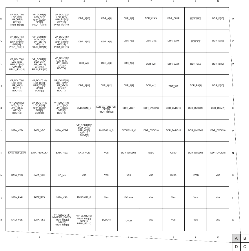 Figure 3-1 Pin Map (Quad A)
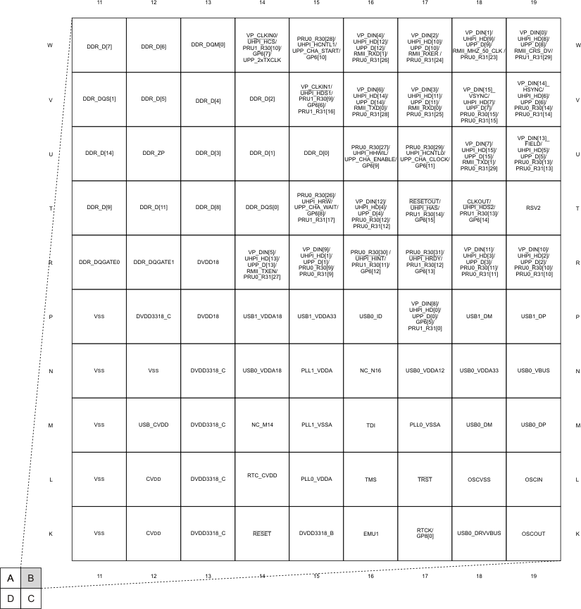 Figure 3-2 Pin Map (Quad B)
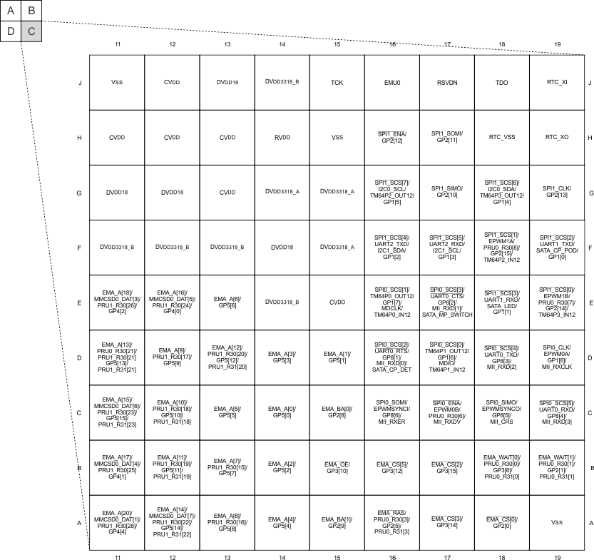 Figure 3-3 Pin Map (Quad C)
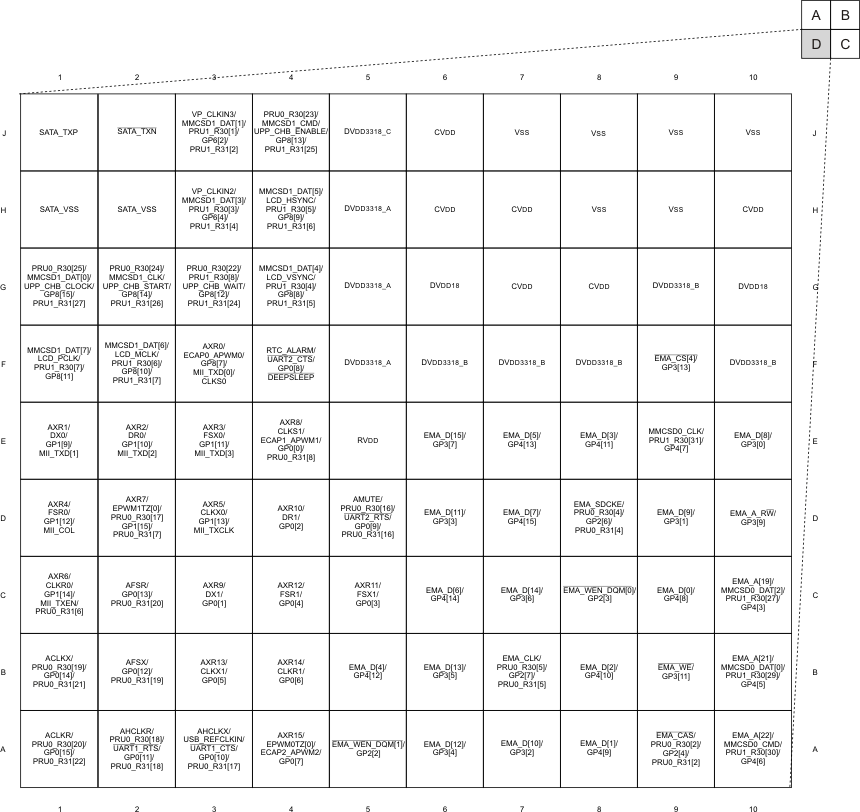 Figure 3-4 Pin Map (Quad D)
3.6 Pin Multiplexing Control
Device level pin multiplexing is controlled by registers PINMUX0 - PINMUX19 in the SYSCFG module.
For the device family, pin multiplexing can be controlled on a pin-by-pin basis. Each pin that is multiplexed with several different functions has a corresponding 4-bit field in one of the PINMUX registers.
Pin multiplexing selects which of several peripheral pin functions controls the pin's IO buffer output data and output enable values only. The default pin multiplexing control for almost every pin is to select 'none' of the peripheral functions in which case the pin's IO buffer is held tri-stated.
Note that the input from each pin is always routed to all of the peripherals that share the pin; the PINMUX registers have no effect on input from a pin.
3.7 Terminal Functions
Table 3-3 to Table 3-29 identify the external signal names, the associated pin/ball numbers along with the mechanical package designator, the pin type (I, O, IO, OZ, or PWR), whether the pin/ball has any internal pullup/pulldown resistors, whether the pin/ball is configurable as an IO in GPIO mode, and a functional pin description.
3.7.1 Device Reset and JTAG
Table 3-3 Reset and JTAG Terminal Functions
| SIGNAL | TYPE(1) | PULL(2) | POWER GROUP(4) |
DESCRIPTION | |
|---|---|---|---|---|---|
| NAME | NO. | ||||
| RESET | |||||
| RESET | K14 | I | IPU | B | Device reset input |
| RESETOUT / UHPI_HAS / PRU1_R30[14] / GP6[15] | T17 | O(3) | CP[21] | C | Reset output |
| JTAG | |||||
| TMS | L16 | I | IPU | B | JTAG test mode select |
| TDI | M16 | I | IPU | B | JTAG test data input |
| TDO | J18 | O | IPU | B | JTAG test data output |
| TCK | J15 | I | IPU | B | JTAG test clock |
| TRST | L17 | I | IPD | B | JTAG test reset |
| EMU0 | J16 | I/O | IPU | B | Emulation pin |
| EMU1 | K16 | I/O | IPU | B | Emulation pin |
| RTCK/ GP8[0] (5) | K17 | I/O | IPD | B | JTAG Test Clock Return Clock Output General-purpose input/output |
Note: For multiplexed pins where functions have different types (ie., input versus output), the table reflects the pin function direction for that particular peripheral.
3.7.2 High-Frequency Oscillator and PLL
Table 3-4 High-Frequency Oscillator and PLL Terminal Functions
| SIGNAL | TYPE(1) | PULL(2) | POWER GROUP(3) |
DESCRIPTION | |
|---|---|---|---|---|---|
| NAME | NO. | ||||
| CLKOUT / UHPI_HDS2 / PRU1_R30[13] / GP6[14] | T18 | O | CP[22] | C | PLL Observation Clock |
| 1.2-V OSCILLATOR | |||||
| OSCIN | L19 | I | — | — | Oscillator input |
| OSCOUT | K19 | O | — | — | Oscillator output |
| OSCVSS | L18 | GND | — | — | Oscillator ground |
| 1.2-V PLL0 | |||||
| PLL0_VDDA | L15 | PWR | — | — | PLL analog VDD (1.2-V filtered supply) |
| PLL0_VSSA | M17 | GND | — | — | PLL analog VSS (for filter) |
| 1.2-V PLL1 | |||||
| PLL1_VDDA | N15 | PWR | — | — | PLL analog VDD (1.2-V filtered supply) |
| PLL1_VSSA | M15 | GND | — | — | PLL analog VSS (for filter) |
Note: For multiplexed pins where functions have different types (ie., input versus output), the table reflects the pin function direction for that particular peripheral.
3.7.3 Real-Time Clock and 32-kHz Oscillator
Table 3-5 Real-Time Clock (RTC) and 1.2-V, 32-kHz Oscillator Terminal Functions
| SIGNAL | TYPE(1) | PULL(2) | POWER GROUP(3) |
DESCRIPTION | |
|---|---|---|---|---|---|
| NAME | NO. | ||||
| RTC_XI | J19 | I | — | — | RTC 32-kHz oscillator input |
| RTC_XO | H19 | O | — | — | RTC 32-kHz oscillator output |
| RTC_ALARM / UART2_CTS / GP0[8] / DEEPSLEEP | F4 | O | CP[0] | A | RTC Alarm |
| RTC_CVDD | L14 | PWR | — | — | RTC module core power (isolated from chip CVDD) |
| RTC_Vss | H18 | GND | — | — | Oscillator ground |
Note: For multiplexed pins where functions have different types (ie., input versus output), the table reflects the pin function direction for that particular peripheral.
3.7.4 DEEPSLEEP Power Control
Table 3-6 DEEPSLEEP Power Control Terminal Functions
| SIGNAL | TYPE(1) | PULL(2) | POWER GROUP(3) |
DESCRIPTION | |
|---|---|---|---|---|---|
| NAME | NO. | ||||
| RTC_ALARM / UART2_CTS / GP0[8] /DEEPSLEEP | F4 | I | CP[0] | A | DEEPSLEEP power control output |
Note: For multiplexed pins where functions have different types (ie., input versus output), the table reflects the pin function direction for that particular peripheral.
3.7.5 External Memory Interface A (EMIFA)
Table 3-7 External Memory Interface A (EMIFA) Terminal Functions
| SIGNAL | TYPE(1) | PULL(2) | POWER GROUP(3) |
DESCRIPTION | |
|---|---|---|---|---|---|
| NAME | NO. | ||||
| EMA_D[15] / GP3[7] | E6 | I/O | CP[17] | B | EMIFA data bus |
| EMA_D[14] / GP3[6] | C7 | I/O | CP[17] | B | |
| EMA_D[13] / GP3[5] | B6 | I/O | CP[17] | B | |
| EMA_D[12] / GP3[4] | A6 | I/O | CP[17] | B | |
| EMA_D[11] / GP3[3] | D6 | I/O | CP[17] | B | |
| EMA_D[10] / GP3[2] | A7 | I/O | CP[17] | B | |
| EMA_D[9] / GP3[1] | D9 | I/O | CP[17] | B | |
| EMA_D[8] / GP3[0] | E10 | I/O | CP[17] | B | |
| EMA_D[7] / GP4[15] | D7 | I/O | CP[17] | B | |
| EMA_D[6] / GP4[14] | C6 | I/O | CP[17] | B | |
| EMA_D[5] / GP4[13] | E7 | I/O | CP[17] | B | |
| EMA_D[4] / GP4[12] | B5 | I/O | CP[17] | B | |
| EMA_D[3] / GP4[11] | E8 | I/O | CP[17] | B | |
| EMA_D[2] / GP4[10] | B8 | I/O | CP[17] | B | |
| EMA_D[1] / GP4[9] | A8 | I/O | CP[17] | B | |
| EMA_D[0] / GP4[8] | C9 | I/O | CP[17] | B | |
| EMA_A[22] / MMCSD0_CMD / PRU1_R30[30] / GP4[6] | A10 | O | CP[18] | B | EMIFA address bus |
| EMA_A[21] / MMCSD0_DAT[0] / PRU1_R30[29] / GP4[5] | B10 | O | CP[18] | B | |
| EMA_A[20] / MMCSD0_DAT[1] / PRU1_R30[28] / GP4[4] | A11 | O | CP[18] | B | |
| EMA_A[19] / MMCSD0_DAT[2] / PRU1_R30[27] / GP4[3] | C10 | O | CP[18] | B | |
| EMA_A[18] / MMCSD0_DAT[3] / PRU1_R30[26] / GP4[2] | E11 | O | CP[18] | B | |
| EMA_A[17] / MMCSD0_DAT[4] / PRU1_R30[25] / GP4[1] | B11 | O | CP[18] | B | |
| EMA_A[16] / MMCSD0_DAT[5] / PRU1_R30[24] / GP4[0] | E12 | O | CP[18] | B | |
| EMA_A[15] / MMCSD0_DAT[6] / PRU1_R30[23] / GP5[15] / PRU1_R31[23] | C11 | O | CP[19] | B | |
| EMA_A[14] / MMCSD0_DAT[7] / PRU1_R30[22] / GP5[14] / PRU1_R31[22] | A12 | O | CP[19] | B | |
| EMA_A[13] /PRU0_R30[21] / PRU1_R30[21] / GP5[13] / PRU1_R31[21] | D11 | O | CP[19] | B | |
| EMA_A[12] / PRU1_R30[20] / GP5[12] / PRU1_R31[20] | D13 | O | CP[19] | B | |
| EMA_A[11] / PRU1_R30[19] / GP5[11] / PRU1_R31[19] | B12 | O | CP[19] | B | EMIFA address bus |
| EMA_A[10] / PRU1_R30[18] / GP5[10] / PRU1_R31[18] | C12 | O | CP[19] | B | |
| EMA_A[9] / PRU1_R30[17] / GP5[9] | D12 | O | CP[19] | B | |
| EMA_A[8] / PRU1_R30[16] / GP5[8] | A13 | O | CP[19] | B | |
| EMA_A[7] / PRU1_R30[15] / GP5[7] | B13 | O | CP[20] | B | |
| EMA_A[6] / GP5[6] | E13 | O | CP[20] | B | |
| EMA_A[5] / GP5[5] | C13 | O | CP[20] | B | |
| EMA_A[4] / GP5[4] | A14 | O | CP[20] | B | |
| EMA_A[3] / GP5[3] | D14 | O | CP[20] | B | |
| EMA_A[2] / GP5[2] | B14 | O | CP[20] | B | |
| EMA_A[1] / GP5[1] | D15 | O | CP[20] | B | |
| EMA_A[0] / GP5[0] | C14 | O | CP[20] | B | |
| EMA_BA[0] / GP2[8] | C15 | O | CP[16] | B | EMIFA bank address |
| EMA_BA[1] / GP2[9] | A15 | O | CP[16] | B | |
| EMA_CLK / PRU0_R30[5] / GP2[7] / PRU0_R31[5] | B7 | O | CP[16] | B | EMIFA clock |
| EMA_SDCKE / PRU0_R30[4] / GP2[6] / PRU0_R31[4] | D8 | O | CP[16] | B | EMIFA SDRAM clock enable |
| EMA_RAS / PRU0_R30[3] / GP2[5] / PRU0_R31[3] | A16 | O | CP[16] | B | EMIFA SDRAM row address strobe |
| EMA_CAS / PRU0_R30[2] / GP2[4] / PRU0_R31[2] | A9 | O | CP[16] | B | EMIFA SDRAM column address strobe |
| EMA_CS[0] / GP2[0] | A18 | O | CP[16] | B | EMIFA SDRAM Chip Select |
| EMA_CS[2] / GP3[15] | B17 | O | CP[16] | B | EMIFA Async Chip Select |
| EMA_CS[3] / GP3[14] | A17 | O | CP[16] | B | |
| EMA_CS[4] / GP3[13] | F9 | O | CP[16] | B | |
| EMA_CS[5] / GP3[12] | B16 | O | CP[16] | B | |
| EMA_A_RW / GP3[9] | D10 | O | CP[16] | B | EMIFA Async Read/Write control |
| EMA_WE / GP3[11] | B9 | O | CP[16] | B | EMIFA SDRAM write enable |
| EMA_WEN_DQM[1] / GP2[2] | A5 | O | CP[16] | B | EMIFA write enable/data mask for EMA_D[15:8] |
| EMA_WEN_DQM[0] / GP2[3] | C8 | O | CP[16] | B | EMIFA write enable/data mask for EMA_D[7:0] |
| EMA_OE / GP3[10] | B15 | O | CP[16] | B | EMIFA output enable |
| EMA_WAIT[0] / PRU0_R30[0] / GP3[8] / PRU0_R31[0] | B18 | I | CP[16] | B | EMIFA wait input/interrupt |
| EMA_WAIT[1] / PRU0_R30[1] / GP2[1] / PRU0_R31[1] | B19 | I | CP[16] | B |
Note: The pin type shown refers to the input, output or high-impedance state of the pin function when configured as the signal name highlighted in bold. All multiplexed signals may enter a high-impedance state when the configured function is input-only or the configured function supports high-Z operation. All GPIO signals can be used as input or output. For multiplexed pins where functions have different types (ie., input versus output), the table reflects the pin function direction for that particular peripheral.
3.7.6 DDR2/mDDR Memory Controller
Table 3-8 DDR2/mDDR Terminal Functions
| SIGNAL | TYPE(1) | PULL(2) | DESCRIPTION | |
|---|---|---|---|---|
| NAME | NO. | |||
| DDR_D[15] | W10 | I/O | IPD | DDR2 SDRAM data bus |
| DDR_D[14] | U11 | I/O | IPD | |
| DDR_D[13] | V10 | I/O | IPD | |
| DDR_D[12] | U10 | I/O | IPD | |
| DDR_D[11] | T12 | I/O | IPD | |
| DDR_D[10] | T10 | I/O | IPD | |
| DDR_D[9] | T11 | I/O | IPD | |
| DDR_D[8] | T13 | I/O | IPD | |
| DDR_D[7] | W11 | I/O | IPD | |
| DDR_D[6] | W12 | I/O | IPD | |
| DDR_D[5] | V12 | I/O | IPD | |
| DDR_D[4] | V13 | I/O | IPD | |
| DDR_D[3] | U13 | I/O | IPD | |
| DDR_D[2] | V14 | I/O | IPD | |
| DDR_D[1] | U14 | I/O | IPD | |
| DDR_D[0] | U15 | I/O | IPD | |
| DDR_A[13] | T5 | O | IPD | DDR2 row/column address |
| DDR_A[12] | V4 | O | IPD | |
| DDR_A[11] | T4 | O | IPD | |
| DDR_A[10] | W4 | O | IPD | |
| DDR_A[9] | T6 | O | IPD | |
| DDR_A[8] | U4 | O | IPD | |
| DDR_A[7] | U6 | O | IPD | |
| DDR_A[6] | W5 | O | IPD | |
| DDR_A[5] | V5 | O | IPD | |
| DDR_A[4] | U5 | O | IPD | |
| DDR_A[3] | V6 | O | IPD | |
| DDR_A[2] | W6 | O | IPD | |
| DDR_A[1] | T7 | O | IPD | |
| DDR_A[0] | U7 | O | IPD | |
| DDR_CLKP | W8 | O | IPD | DDR2 clock (positive) |
| DDR_CLKN | W7 | O | IPD | DDR2 clock (negative) |
| DDR_CKE | V7 | O | IPD | DDR2 clock enable |
| DDR_WE | T8 | O | IPD | DDR2 write enable |
| DDR_RAS | W9 | O | IPD | DDR2 row address strobe |
| DDR_CAS | U9 | O | IPD | DDR2 column address strobe |
| DDR_CS | V9 | O | IPD | DDR2 chip select |
| DDR_DQM[0] | W13 | O | IPD | DDR2 data mask outputs |
| DDR_DQM[1] | R10 | O | IPD | |
| DDR_DQS[0] | T14 | I/O | IPD | DDR2 data strobe inputs/outputs |
| DDR_DQS[1] | V11 | I/O | IPD | |
| DDR_BA[2] | U8 | O | IPD | DDR2 SDRAM bank address |
| DDR_BA[1] | T9 | O | IPD | |
| DDR_BA[0] | V8 | O | IPD | |
| DDR_DQGATE0 | R11 | O | IPD | DDR2 loopback signal for external DQS gating. Route to DDR and back to DDR_DQGATE1 with same constraints as used for DDR clock and data. |
| DDR_DQGATE1 | R12 | I | IPD | DDR2 loopback signal for external DQS gating. Route to DDR and back to DDR_DQGATE0 with same constraints as used for DDR clock and data. |
| DDR_ZP | U12 | O | — | DDR2 reference output for drive strength calibration of N and P channel outputs. Tie to ground via 50 ohm resistor @ 5% tolerance. |
| DDR_VREF | R6 | I | — | DDR voltage input for the DDR2/mDDR I/O buffers. Note even in the case of mDDR an external resistor divider connected to this pin is necessary. |
| DDR_DVDD18 | N10, P10, N9, P9, R9, P8, R8, P7, R7, N6 | PWR | — | DDR PHY 1.8V power supply pins |
Note: The pin type shown refers to the input, output or high-impedance state of the pin function when configured as the signal name highlighted in bold. All multiplexed signals may enter a high-impedance state when the configured function is input-only or the configured function supports high-Z operation. All GPIO signals can be used as input or output. For multiplexed pins where functions have different types (ie., input versus output), the table reflects the pin function direction for that particular peripheral.
3.7.7 Serial Peripheral Interface Modules (SPI)
Table 3-9 Serial Peripheral Interface (SPI) Terminal Functions
| SIGNAL | TYPE(1) | PULL(2) | POWER GROUP(3) |
DESCRIPTION | |
|---|---|---|---|---|---|
| NAME | NO. | ||||
| SPI0 | |||||
| SPI0_CLK / EPWM0A / GP1[8] / MII_RXCLK | D19 | I/O | CP[7] | A | SPI0 clock |
| SPI0_ENA / EPWM0B / PRU0_R30[6] / MII_RXDV | C17 | I/O | CP[7] | A | SPI0 enable |
| SPI0_SCS[0] / TM64P1_OUT12 / GP1[6] / MDIO / TM64P1_IN12 | D17 | I/O | CP[10] | A | SPI0 chip selects |
| SPI0_SCS[1] / TM64P0_OUT12 / GP1[7] / MDCLK / TM64P0_IN12 | E16 | I/O | CP[10] | A | |
| SPI0_SCS[2] / UART0_RTS / GP8[1]/ MII_RXD[0] / SATA_CP_DET | D16 | I/O | CP[9] | A | |
| SPI0_SCS[3] / UART0_CTS / GP8[2] / MII_RXD[1] / SATA_MP_SWITCH | E17 | I/O | CP[9] | A | |
| SPI0_SCS[4] / UART0_TXD / GP8[3] / MII_RXD[2] | D18 | I/O | CP[8] | A | |
| SPI0_SCS[5] / UART0_RXD / GP8[4] / MII_RXD[3] | C19 | I/O | CP[8] | A | |
| SPI0_SIMO / EPWMSYNCO / GP8[5] / MII_CRS | C18 | I/O | CP[7] | A | SPI0 data slave-in-master-out |
| SPI0_SOMI / EPWMSYNCI / GP8[6] / MII_RXER | C16 | I/O | CP[7] | A | SPI0 data slave-out-master-in |
| SPI1 | |||||
| SPI1_CLK / GP2[13] | G19 | I/O | CP[15] | A | SPI1 clock |
| SPI1_ENA / GP2[12] | H16 | I/O | CP[15] | A | SPI1 enable |
| SPI1_SCS[0] / EPWM1B / PRU0_R30[7] / GP2[14] / TM64P3_IN12 | E19 | I/O | CP[14] | A | SPI1 chip selects |
| SPI1_SCS[1] / EPWM1A / PRU0_R30[8] / GP2[15] / TM64P2_IN12 | F18 | I/O | CP[14] | A | |
| SPI1_SCS[2] / UART1_TXD / SATA_CP_POD / GP1[0] | F19 | I/O | CP[13] | A | |
| SPI1_SCS[3] / UART1_RXD / SATA_LED / GP1[1] | E18 | I/O | CP[13] | A | |
| SPI1_SCS[4] / UART2_TXD / I2C1_SDA /GP1[2] | F16 | I/O | CP[12] | A | |
| SPI1_SCS[5] / UART2_RXD / I2C1_SCL /GP1[3] | F17 | I/O | CP[12] | A | |
| SPI1_SCS[6] / I2C0_SDA / TM64P3_OUT12 / GP1[4] | G18 | I/O | CP[11] | A | |
| SPI1_SCS[7] / I2C0_SCL / TM64P2_OUT12 / GP1[5] | G16 | I/O | CP[11] | A | |
| SPI1_SIMO / GP2[10] | G17 | I/O | CP[15] | A | SPI1 data slave-in-master-out |
| SPI1_SOMI / GP2[11] | H17 | I/O | CP[15] | A | SPI1 data slave-out-master-in |
Note: The pin type shown refers to the input, output or high-impedance state of the pin function when configured as the signal name highlighted in bold. All multiplexed signals may enter a high-impedance state when the configured function is input-only or the configured function supports high-Z operation. All GPIO signals can be used as input or output. For multiplexed pins where functions have different types (ie., input versus output), the table reflects the pin function direction for that particular peripheral.
3.7.8 PROFIBUS Real-Time Unit (PRU)
Table 3-10 PROFIBUS Real-Time Unit (PRU) Terminal Functions
| SIGNAL | TYPE(1) | PULL(2) | POWER GROUP(3) |
DESCRIPTION | |
|---|---|---|---|---|---|
| NAME | NO. | ||||
| PRU0 Signals | |||||
| PRU0_R30[31] / UHPI_HRDY / PRU1_R30[12] / GP6[13] | R17 | O | CP[23] | C | PRU0 Output Signals |
| PRU0_R30[30] / UHPI_HINT / PRU1_R30[11] / GP6[12] | R16 | O | CP[23] | C | |
| PRU0_R30[29] / UHPI_HCNTL0 / UPP_CHA_CLOCK / GP6[11] | U17 | O | CP[24] | C | |
| PRU0_R30[28] / UHPI_HCNTL1 / UPP_CHA_START / GP6[10] | W15 | O | CP[24] | C | |
| PRU0_R30[27] / UHPI_HHWIL / UPP_CHA_ENABLE / GP6[9] | U16 | O | CP[24] | C | |
| PRU0_R30[26] / UHPI_HRW / / UPP_CHA_WAITGP6[8] / PRU1_R31[17] | T15 | O | CP[24] | C | |
| PRU0_R30[25] / MMCSD1_DAT[0] / UPP_CHB_CLOCK / GP8[15] / PRU1_R31[27] | G1 | O | CP30] | C | |
| PRU0_R30[24] / MMCSD1_CLK / UPP_CHB_START / GP8[14] / PRU1_R31[26] | G2 | O | CP[30] | C | |
| PRU0_R30[23] / MMCSD1_CMD / UPP_CHB_ENABLE / GP8[13] / PRU1_R31[25] | J4 | O | CP[30] | C | |
| PRU0_R30[22] / PRU1_R30[8] / UPP_CHB_WAIT / GP8[12] / PRU1_R31[24] | G3 | O | CP[30] | C | |
| EMA_A[13] / PRU0_R30[21] / PRU1_R30[21] / GP5[13] / PRU1_R31[21] | D11 | O | CP[19] | B | |
| ACLKR / PRU0_R30[20] / GP0[15] / PRU0_R31[22] | A1 | O | CP[0] | A | |
| ACLKX / PRU0_R30[19] / GP0[14] / PRU0_R31[21] | B1 | O | CP[0] | A | |
| AHCLKR / PRU0_R30[18] / UART1_RTS / GP0[11] / PRU0_R31[18] | A2 | O | CP[0] | A | |
| AXR7 / EPWM1TZ[0] / PRU0_R30[17] / GP1[15] / PRU0_R31[7] | D2 | O | CP[4] | A | |
| AMUTE / PRU0_R30[16] / UART2_RTS / GP0[9] / PRU0_R31[16] | D5 | O | CP[0] | A | |
| VP_DIN[15]_VSYNC / UHPI_HD[7] / UPP_D[7] / PRU0_R30[15] / PRU0_R31[15] | V18 | O | CP[27] | C | |
| VP_DIN[14]_HSYNC / UHPI_HD[6] / UPP_D[6] / PRU0_R30[14] / PRU0_R31[14] | V19 | O | CP[27] | C | |
| VP_DIN[13]_FIELD / UHPI_HD[5] / UPP_D[5] / PRU0_R30[13] / PRU0_R31[13] | U19 | O | CP[27] | C | |
| VP_DIN[12] / UHPI_HD[4] / UPP_D[4] / PRU0_R30[12] / PRU0_R31[12] | T16 | O | CP[27] | C | |
| VP_DIN[11] / UHPI_HD[3] / UPP_D[3] / PRU0_R30[11] / PRU0_R31[11] | R18 | O | CP[27] | C | |
| VP_DIN[10] / UHPI_HD[2] / UPP_D[2] / PRU0_R30[10] / PRU0_R31[10] | R19 | O | CP[27] | C | |
| VP_DIN[9] / UHPI_HD[1] / UPP_D[1] / PRU0_R30[9] / PRU0_R31[9] | R15 | O | CP[27] | C | |
| SPI1_SCS[1] / EPWM1A / PRU0_R30[8] / GP2[15] / TM64P2_IN12 | F18 | O | CP[14] | A | |
| SPI1_SCS[0] / EPWM1B / PRU0_R30[7] / GP2[14] / TM64P3_IN12 | E19 | O | CP[14] | A | |
| SPI0_ENA / EPWM0B / PRU0_R30[6] / MII_RXDV | C17 | O | CP[7] | A | |
| EMA_CLK / PRU0_R30[5] / GP2[7] / PRU0_R31[5] | B7 | O | CP[16] | B | PRU0 Output Signals |
| EMA_SDCKE / PRU0_R30[4] / GP2[6] / PRU0_R31[4] | D8 | O | CP[16] | B | |
| EMA_RAS / PRU0_R30[3] / GP2[5] / PRU0_R31[3] | A16 | O | CP[16] | B | |
| EMA_CAS / PRU0_R30[2] / GP2[4] / PRU0_R31[2] | A9 | O | CP[16] | B | |
| EMA_WAIT[1] / PRU0_R30[1] / GP2[1] / PRU0_R31[1] | B19 | O | CP[16] | B | |
| EMA_WAIT[0] / PRU0_R30[0] / GP3[8] / PRU0_R31[0] | B18 | O | CP[16] | B | |
| VP_DIN[7] / UHPI_HD[15] / UPP_D[15] / RMII_TXD[1] / PRU0_R31[29] | U18 | I | CP[26] | C | PRU0 Input Signals |
| VP_DIN[6] / UHPI_HD[14] / UPP_D[14] / RMII_TXD[0] / PRU0_R31[28] | V16 | I | CP[26] | C | |
| VP_DIN[5] / UHPI_HD[13] / UPP_D[13] / RMII_TXEN / PRU0_R31[27] | R14 | I | CP[26] | C | |
| VP_DIN[4] / UHPI_HD[12] / UPP_D[12] / RMII_RXD[1] / PRU0_R31[26] | W16 | I | CP[26] | C | |
| VP_DIN[3] / UHPI_HD[11] / UPP_D[11] / RMII_RXD[0] / PRU0_R31[25] | V17 | I | CP[26] | C | |
| VP_DIN[2] / UHPI_HD[10] / UPP_D[10] / RMII_RXER / PRU0_R31[24] | W17 | I | CP[26] | C | |
| VP_DIN[1] / UHPI_HD[9]UPP_D[9] / RMII_MHZ_50_CLK / PRU0_R31[23] | W18 | I | CP[26] | C | |
| ACLKR / PRU0_R30[20] / GP0[15] / PRU0_R31[22] | A1 | I | CP[0] | A | |
| ACLKX / PRU0_R30[19] / GP0[14] / PRU0_R31[21] | B1 | I | CP[0] | A | |
| AFSR / GP0[13] / PRU0_R31[20] | C2 | I | CP[0] | A | |
| AFSX / GP0[12] / PRU0_R31[19] | B2 | I | CP[0] | A | |
| AHCLKR / PRU0_R30[18] / UART1_RTS / GP0[11] / PRU0_R31[18] | A2 | I | CP[0] | A | |
| AHCLKX / USB_REFCLKIN / UART1_CTS / GP0[10] / PRU0_R31[17] | A3 | I | CP[0] | A | |
| AMUTE / PRU0_R30[16] / UART2_RTS / GP0[9] / PRU0_R31[16] | D5 | I | CP[0] | A | |
| VP_DIN[15]_VSYNC / UHPI_HD[7] / UPP_D[7] / PRU0_R30[15] / PRU0_R31[15] | V18 | I | CP[27] | C | |
| VP_DIN[14]_HSYNC / UHPI_HD[6] / UPP_D[6] / PRU0_R30[14] / PRU0_R31[14] | V19 | I | CP[27] | C | |
| VP_DIN[13]_FIELD / UHPI_HD[5] / UPP_D[5] / PRU0_R30[13] / PRU0_R31[13] | U19 | I | CP[27] | C | |
| VP_DIN[12] / UHPI_HD[4] / UPP_D[4] / PRU0_R30[12] / PRU0_R31[12] | T16 | I | CP[27] | C | |
| VP_DIN[11] / UHPI_HD[3] / UPP_D[3] / PRU0_R30[11] / PRU0_R31[11] | R18 | I | CP[27] | C | |
| VP_DIN[10] / UHPI_HD[2] / UPP_D[2] / PRU0_R30[10] / PRU0_R31[10] | R19 | I | CP[27] | C | |
| VP_DIN[9] / UHPI_HD[1] / UPP_D[1] / PRU0_R30[9] / PRU0_R31[9] | R15 | I | CP[27] | C | |
| AXR8 / CLKS1 / ECAP1_APWM1 / GP0[0] / PRU0_R31[8] | E4 | I | CP[3] | A | |
| AXR7 / EPWM1TZ[0] / PRU0_R30[17] / GP1[15] / PRU0_R31[7] | D2 | I | CP[4] | A | |
| AXR6 / CLKR0 / GP1[14] / MII_TXEN / PRU0_R31[6] | C1 | I | CP[5] | A | |
| EMA_CLK / PRU0_R30[5] / GP2[7] / PRU0_R31[5] | B7 | I | CP[16] | B | |
| EMA_SDCKE / PRU0_R30[4] / GP2[6] / PRU0_R31[4] | D8 | I | CP[16] | B | |
| EMA_RAS / PRU0_R30[3] / GP2[5] / PRU0_R31[3] | A16 | I | CP[16] | B | |
| EMA_CAS / PRU0_R30[2] / GP2[4] / PRU0_R31[2] | A9 | I | CP[16] | B | |
| EMA_WAIT[1] / PRU0_R30[1] / GP2[1] / PRU0_R31[1] | B19 | I | CP[16] | B | |
| EMA_WAIT[0] / PRU0_R30[0] / GP3[8] / PRU0_R31[0] | B18 | I | CP[16] | B | |
| PRU1 Signals | |||||
| MMCSD0_CLK / PRU1_R30[31] /GP4[7] | E9 | O | CP[18] | B | PRU1 Output Signals |
| EMA_A[22] / MMCSD0_CMD / PRU1_R30[30] / GP4[6] | A10 | O | CP[18] | B | |
| EMA_A[21] / MMCSD0_DAT[0] / PRU1_R30[29] / GP4[5] | B10 | O | CP[18] | B | |
| EMA_A[20] / MMCSD0_DAT[1] / PRU1_R30[28] / GP4[4] | A11 | O | CP[18] | B | |
| EMA_A[19] / MMCSD0_DAT[2] / PRU1_R30[27] / GP4[3] | C10 | O | CP[18] | B | |
| EMA_A[18] / MMCSD0_DAT[3] / PRU1_R30[26] / GP4[2] | E11 | O | CP[18] | B | |
| EMA_A[17] / MMCSD0_DAT[4] / PRU1_R30[25] / GP4[1] | B11 | O | CP[18] | B | |
| EMA_A[16] / MMCSD0_DAT[5] / PRU1_R30[24] / GP4[0] | E12 | O | CP[18] | B | |
| EMA_A[15] / MMCSD0_DAT[6] / PRU1_R30[23] / GP5[15] / PRU1_R31[23] | C11 | O | CP[19] | B | |
| EMA_A[14] / MMCSD0_DAT[7] / PRU1_R30[22] / GP5[14] / PRU1_R31[22] | A12 | O | CP[19] | B | |
| EMA_A[13] / PRU0_R30[21] / PRU1_R30[21] / GP5[13] / PRU1_R31[21] | D11 | O | CP[19] | B | |
| EMA_A[12] / PRU1_R30[20] / GP5[12] / PRU1_R31[20] | D13 | O | CP[19] | B | |
| EMA_A[11] / PRU1_R30[19] / GP5[11] / PRU1_R31[19] | B12 | O | CP[19] | B | |
| EMA_A[10] / PRU1_R30[18] / GP5[10] / PRU1_R31[18] | C12 | O | CP[19] | B | |
| EMA_A[9] / PRU1_R30[17] / GP5[9] | D12 | O | CP[19] | B | |
| EMA_A[8] / PRU1_R30[16] / GP5[8] | A13 | O | CP[19] | B | |
| EMA_A[7] / PRU1_R30[15] / GP5[7] | B13 | O | CP[20] | B | |
| RESETOUT / UHPI_HAS / PRU1_R30[14] / GP6[15] | T17 | O | CP[21] | C | |
| CLKOUT / UHPI_HDS2 / PRU1_R30[13] / GP6[14] | T18 | O | CP[22] | C | |
| PRU0_R30[31] / UHPI_HRDY / PRU1_R30[12] / GP6[13] | R17 | O | CP[23] | C | |
| PRU0_R30[30] / UHPI_HINT / PRU1_R30[11] / GP6[12] | R16 | O | CP[23] | C | |
| VP_CLKIN0 / UHPI_HCS / PRU1_R30[10] / GP6[7] / UPP_2xTXCLK | W14 | O | CP[25] | C | |
| VP_CLKIN1 / UHPI_HDS1 / PRU1_R30[9] / GP6[6] / PRU1_R31[16] | V15 | O | CP[25] | C | |
| PRU0_R30[22] / PRU1_R30[8] / UPP_CHB_WAIT / GP8[12] / PRU1_R31[24] | G3 | O | CP[30] | C | |
| MMCSD1_DAT[7] / LCD_PCLK / PRU1_R30[7] / GP8[11] | F1 | O | CP[31] | C | |
| MMCSD1_DAT[6] / LCD_MCLK / PRU1_R30[6] / GP8[10] / PRU1_R31[7] | F2 | O | CP[31] | C | |
| MMCSD1_DAT[5] / LCD_HSYNC / PRU1_R30[5] / GP8[9] / PRU1_R31[6] | H4 | O | CP[31] | C | |
| MMCSD1_DAT[4] / LCD_VSYNC / PRU1_R30[4] / GP8[8] / PRU1_R31[5] | G4 | O | CP[31] | C | |
| VP_CLKIN2 / MMCSD1_DAT[3] / PRU1_R30[3] / GP6[4] / PRU1_R31[4] | H3 | O | CP[30] | C | |
| VP_CLKOUT2 / MMCSD1_DAT[2] / PRU1_R30[2] / GP6[3] / PRU1_R31[3] | K3 | O | CP[30] | C | |
| VP_CLKIN3 / MMCSD1_DAT[1] / PRU1_R30[1] / GP6[2] / PRU1_R31[2] | J3 | O | CP[30] | C | |
| VP_CLKOUT3 / PRU1_R30[0] / GP6[1] / PRU1_R31[1] | K4 | O | CP[30] | C | |
| VP_DIN[0] / UHPI_HD[8] / UPP_D[8] / RMII_CRS_DV / PRU1_R31[29] | W19 | I | CP[26] | C | PRU1 Input Signals |
| LCD_AC_ENB_CS / GP6[0] / PRU1_R31[28] | R5 | I | CP[31] | C | |
| PRU0_R30[25] / MMCSD1_DAT[0] / UPP_CHB_CLOCK / GP8[15] / PRU1_R31[27] | G1 | I | CP[30] | C | |
| PRU0_R30[24] / MMCSD1_CLK / UPP_CHB_START / GP8[14] / PRU1_R31[26] | G2 | I | CP[30] | C | |
| PRU0_R30[23] / MMCSD1_CMD / UPP_CHB_ENABLE / GP8[13] / PRU1_R31[25] | J4 | I | CP[30] | C | |
| PRU0_R30[22] / PRU1_R30[8] / UPP_CHB_WAIT / GP8[12] / PRU1_R31[24] | G3 | I | CP[30] | C | |
| EMA_A[15] / MMCSD0_DAT[6] / PRU1_R30[23] / GP[15] / PRU1_R31[23] | C11 | I | CP[19] | B | |
| EMA_A[14] / MMCSD0_DAT[7] / PRU1_R30[22] /GP[14] / PRU1_R31[22] | A12 | I | CP[19] | B | |
| EMA_A[13] / PRU0_R30[21] / PRU1_R30[21] /GP[13] / PRU1_R31[21] | D11 | I | CP[19] | B | |
| EMA_A[12] / PRU1_R30[20] / GP[12] / PRU1_R31[20] | D13 | I | CP[19] | B | |
| EMA_A[11] / PRU1_R30[19] /GP[11] / PRU1_R31[19] | B12 | I | CP[19] | B | |
| EMA_A[10] / PRU1_R30[18] /GP[10] / PRU1_R31[18] | C12 | I | CP[19] | B | |
| PRU0_R30[26] / UHPI_HRW / UPP_CHA_WAIT / GP6[8] / PRU1_R31[17] | T15 | I | CP[24] | C | |
| VP_CLKIN1 / UHPI_HDS1 / PRU1_R30[9] / GP6[6] / PRU1_R31[16] | V15 | I | CP[25] | C | |
| VP_DOUT[7] / LCD_D[7] / UPP_XD[15] / GP7[15] / PRU1_R31[15] | U2 | I | CP[28] | C | |
| VP_DOUT[6] / LCD_D[6] / UPP_XD[14] / GP7[14] / PRU1_R31[14] | U1 | I | CP[28] | C | |
| VP_DOUT[5] / LCD_D[5] / UPP_XD[13] / GP7[13] / PRU1_R31[13] | V3 | I | CP[28] | C | |
| VP_DOUT[4] / LCD_D[4] / UPP_XD[12] / GP7[12] / PRU1_R31[12] | V2 | I | CP[28] | C | |
| VP_DOUT[3] / LCD_D[3] / UPP_XD[11] / GP7[11] / PRU1_R31[11] | V1 | I | CP[28] | C | |
| VP_DOUT[2] / LCD_D[2] / UPP_XD[10] / GP7[10] / PRU1_R31[10] | W3 | I | CP[28] | C | |
| VP_DOUT[1] / LCD_D[1] / UPP_XD[9] / GP7[9] / PRU1_R31[9] | W2 | I | CP[28] | C | |
| VP_DOUT[0] / LCD_D[0] / UPP_XD[8] / GP7[8] / PRU1_R31[8] | W1 | I | CP[28] | C | |
| MMCSD1_DAT[6] / LCD_MCLK / PRU1_R30[6] / GP8[10] / PRU1_R31[7] | F2 | I | CP[31] | C | |
| MMCSD1_DAT[5] / LCD_HSYNC / PRU1_R30[5] / GP8[9] / PRU1_R31[6] | H4 | I | CP[31] | C | |
| MMCSD1_DAT[4] / LCD_VSYNC / PRU1_R30[4] / GP8[8] / PRU1_R31[5] | G4 | I | CP[31] | C | |
| VP_CLKIN2 / MMCSD1_DAT[3] / PRU1_R30[3] / GP6[4] / PRU1_R31[4] | H3 | I | CP[30] | C | |
| VP_CLKOUT2 / MMCSD1_DAT[2] / PRU1_R30[2] / GP6[3] / PRU1_R31[3] | K3 | I | CP[30] | C | |
| VP_CLKIN3 / MMCSD1_DAT[1] / PRU1_R30[1] / GP6[2] / PRU1_R31[2] | J3 | I | CP[30] | C | |
| VP_CLKOUT3 / PRU1_R30[0] / GP6[1] / PRU1_R31[1] | K4 | I | CP[30] | C | |
| VP_DIN[8] / UHPI_HD[0] / UPP_D[0] / GP6[5] / PRU1_R31[0] | P17 | I | CP[27] | C | |
3.7.9 Enhanced Capture/Auxiliary PWM Modules (eCAP0)
The eCAP Module pins function as either input captures or auxiliary PWM 32-bit outputs, depending upon how the eCAP module is programmed.
Table 3-11 Enhanced Capture Module (eCAP) Terminal Functions
| SIGNAL | TYPE(1) | PULL(2) | POWER GROUP(3) |
DESCRIPTION | ||
|---|---|---|---|---|---|---|
| NAME | NO. | |||||
| eCAP0 | ||||||
| AXR0 / ECAP0_APWM0 / GP8[7] / MII_TXD[0] / CLKS0 | F3 | I/O | CP[6] | A | enhanced capture 0 input or auxiliary PWM 0 output |
|
| eCAP1 | ||||||
| AXR8 / CLKS1 / ECAP1_APWM1 / GP0[0] / PRU0_R31[8] | E4 | I/O | CP[3] | A | enhanced capture 1 input or auxiliary PWM 1 output |
|
| eCAP2 | ||||||
| AXR15 / EPWM0TZ[0] / ECAP2_APWM2 / GP0[7] | A4 | I/O | CP[1] | A | enhanced capture 2 input or auxiliary PWM 2 output |
|
Note: The pin type shown refers to the input, output or high-impedance state of the pin function when configured as the signal name highlighted in bold. All multiplexed signals may enter a high-impedance state when the configured function is input-only or the configured function supports high-Z operation. All GPIO signals can be used as input or output. For multiplexed pins where functions have different types (ie., input versus output), the table reflects the pin function direction for that particular peripheral.
3.7.10 Enhanced Pulse Width Modulators (eHRPWM)
Table 3-12 Enhanced Pulse Width Modulator (eHRPWM) Terminal Functions
| SIGNAL | TYPE(1) | PULL(2) | POWER GROUP(3) |
DESCRIPTION | |
|---|---|---|---|---|---|
| NAME | NO. | ||||
| eHRPWM0 | |||||
| SPI0_CLK / EPWM0A / GP1[8] / MII_RXCLK | D19 | I/O | CP[7] | A | eHRPWM0 A output (with high-resolution) |
| SPI0_ENA / EPWM0B / PRU0_R30[6] / MII_RXDV | C17 | I/O | CP[7] | A | eHRPWM0 B output |
| AXR15 / EPWM0TZ[0] / ECAP2_APWM2 / GP0[7] | A4 | I | CP[1] | A | eHRPWM0 trip zone input |
| SPI0_SOMI / EPWMSYNCI / GP8[6] / MII_RXER | C16 | I | CP[7] | A | eHRPWM0 sync input |
| SPI0_SIMO / EPWMSYNCO / GP8[5] / MII_CRS | C18 | I/O | CP[7] | A | eHRPWM0 sync output |
| eHRPWM1 | |||||
| SPI1_SCS[1] / EPWM1A / PRU0_R30[8] / GP2[15] / TM64P2_IN12 | F18 | I/O | CP[14] | A | eHRPWM1 A output (with high-resolution) |
| SPI1_SCS[0] / EPWM1B / PRU0_R30[7] / GP2[14] / TM64P3_IN12 | E19 | I/O | CP[14] | A | eHRPWM1 B output |
| AXR7 / EPWM1TZ[0] / PRU0_R30[17] / GP1[15] / PRU0_R31[7] | D2 | I | CP[4] | A | eHRPWM1 trip zone input |
Note: The pin type shown refers to the input, output or high-impedance state of the pin function when configured as the signal name highlighted in bold. All multiplexed signals may enter a high-impedance state when the configured function is input-only or the configured function supports high-Z operation. All GPIO signals can be used as input or output. For multiplexed pins where functions have different types (ie., input versus output), the table reflects the pin function direction for that particular peripheral.
3.7.11 Boot
Table 3-13 Boot Mode Selection Terminal Functions(3)
| SIGNAL | TYPE(1) | PULL(2) | POWER GROUP(4) |
DESCRIPTION | |
|---|---|---|---|---|---|
| NAME | NO. | ||||
| VP_DOUT[15] / LCD_D[15] / UPP_XD[7] /GP7[7] / BOOT[7] | P4 | I | CP[29] | C | Boot Mode Selection Pins |
| VP_DOUT[14] / LCD_D[14] / UPP_XD[6] /GP7[6] / BOOT[6] | R3 | I | CP[29] | C | |
| VP_DOUT[13] / LCD_D[13] / UPP_XD[5] /GP7[5] / BOOT[5] | R2 | I | CP[29] | C | |
| VP_DOUT[12] / LCD_D[12] / UPP_XD[4] / GP7[4] / BOOT[4] | R1 | I | CP[29] | C | |
| VP_DOUT[11] / LCD_D[11] / UPP_XD[3] /GP7[3] / BOOT[3] | T3 | I | CP[29] | C | |
| VP_DOUT[10] / LCD_D[10] / UPP_XD[2] /GP7[2] / BOOT[2] | T2 | I | CP[29] | C | |
| VP_DOUT[9] / LCD_D[9] / UPP_XD[1] /GP7[1] / BOOT[1] | T1 | I | CP[29] | C | |
| VP_DOUT[8] / LCD_D[8] / UPP_XD[0] /GP7[0] / BOOT[0] | U3 | I | CP[29] | C |
Note: The pin type shown refers to the input, output or high-impedance state of the pin function when configured as the signal name highlighted in bold. All multiplexed signals may enter a high-impedance state when the configured function is input-only or the configured function supports high-Z operation. All GPIO signals can be used as input or output. For multiplexed pins where functions have different types (ie., input versus output), the table reflects the pin function direction for that particular peripheral.
3.7.12 Universal Asynchronous Receiver/Transmitters (UART0, UART1, UART2)
Table 3-14 Universal Asynchronous Receiver/Transmitter (UART) Terminal Functions
| SIGNAL | TYPE(1) | PULL(2) | POWER GROUP(3) |
DESCRIPTION | |
|---|---|---|---|---|---|
| NAME | NO. | ||||
| UART0 | |||||
| SPI0_SCS[5] / UART0_RXD / GP8[4] / MII_RXD[3] | C19 | I | CP[8] | A | UART0 receive data |
| SPI0_SCS[4] / UART0_TXD / GP8[3] / MII_RXD[2] | D18 | O | CP[8] | A | UART0 transmit data |
| SPI0_SCS[2] / UART0_RTS / GP8[1] / MII_RXD[0] / SATA_CP_DET | D16 | O | CP[9] | A | UART0 ready-to-send output |
| SPI0_SCS[3] / UART0_CTS / GP8[2] / MII_RXD[1] / SATA_MP_SWITCH | E17 | I | CP[9] | A | UART0 clear-to-send input |
| UART1 | |||||
| SPI1_SCS[3] / UART1_RXD / SATA_LED / GP1[1] | E18 | I | CP[13] | A | UART1 receive data |
| SPI1_SCS[2] / UART1_TXD / SATA_CP_POD / GP1[0] | F19 | O | CP[13] | A | UART1 transmit data |
| AHCLKR / PRU0_R30[18] / UART1_RTS / GP0[11] / PRU0_R31[18] | A2 | O | CP[0] | A | UART1 ready-to-send output |
| AHCLKX / USB_REFCLKIN / UART1_CTS / GP0[10] / PRU0_R31[17] |
A3 | I | CP[0] | A | UART1 clear-to-send input |
| UART2 | |||||
| SPI1_SCS[5] / UART2_RXD / I2C1_SCL / GP1[3] | F17 | I | CP[12] | A | UART2 receive data |
| SPI1_SCS[4] / UART2_TXD / I2C1_SDA / GP1[2] | F16 | O | CP[12] | A | UART2 transmit data |
| AMUTE / PRU0_R30[16] / UART2_RTS / GP0[9] / PRU0_R31[16] | D5 | O | CP[0] | A | UART2 ready-to-send output |
| RTC_ALARM / UART2_CTS / GP0[8] / DEEPSLEEP | F4 | I | CP[0] | A | UART2 clear-to-send input |
Note: The pin type shown refers to the input, output or high-impedance state of the pin function when configured as the signal name highlighted in bold. All multiplexed signals may enter a high-impedance state when the configured function is input-only or the configured function supports high-Z operation. All GPIO signals can be used as input or output. For multiplexed pins where functions have different types (ie., input versus output), the table reflects the pin function direction for that particular peripheral.
3.7.13 Inter-Integrated Circuit Modules(I2C0, I2C1)
Table 3-15 Inter-Integrated Circuit (I2C) Terminal Functions
| SIGNAL | TYPE(1) | PULL(2) | POWER GROUP(3) |
DESCRIPTION | |
|---|---|---|---|---|---|
| NAME | NO. | ||||
| I2C0 | |||||
| SPI1_SCS[6] / I2C0_SDA / TM64P3_OUT12 / GP1[4] | G18 | I/O | CP[11] | A | I2C0 serial data |
| SPI1_SCS[7] / I2C0_SCL / TM64P2_OUT12 / GP1[5] | G16 | I/O | CP[11] | A | I2C0 serial clock |
| I2C1 | |||||
| SPI1_SCS[4] / UART2_TXD / I2C1_SDA / GP1[2] | F16 | I/O | CP[12] | A | I2C1 serial data |
| SPI1_SCS[5] / UART2_RXD / I2C1_SCL / GP1[3] | F17 | I/O | CP[12] | A | I2C1 serial clock |
Note: The pin type shown refers to the input, output or high-impedance state of the pin function when configured as the signal name highlighted in bold. All multiplexed signals may enter a high-impedance state when the configured function is input-only or the configured function supports high-Z operation. All GPIO signals can be used as input or output. For multiplexed pins where functions have different types (ie., input versus output), the table reflects the pin function direction for that particular peripheral.
3.7.14 Timers
Table 3-16 Timers Terminal Functions
| SIGNAL | TYPE(1) | PULL(2) | POWER GROUP(3) |
DESCRIPTION | ||
|---|---|---|---|---|---|---|
| NAME | NO. | |||||
| TIMER0 | ||||||
| SPI0_SCS[1] /TM64P0_OUT12 / GP1[7] / MDCLK /TM64P0_IN12 | E16 | I | CP[10] | A | Timer0 lower input | |
| SPI0_SCS[1] / TM64P0_OUT12 / GP1[7] / MDCLK / TM64P0_IN12 | E16 | O | CP[10] | A | Timer0 lower output | |
| TIMER1 (Watchdog) | ||||||
| SPI0_SCS[0] / TM64P1_OUT12 / GP1[6] / MDIO /TM64P1_IN12 | D17 | I | CP[10] | A | Timer1 lower input | |
| SPI0_SCS[0] / TM64P1_OUT12 / GP1[6] / MDIO /TM64P1_IN12 | D17 | O | CP[10] | A | Timer1 lower output | |
| TIMER2 | ||||||
| SPI1_SCS[1] / EPWM1A / PRU0_R30[8] / GP2[15] / TM64P2_IN12 | F18 | I | CP[14] | A | Timer2 lower input | |
| SPI1_SCS[7] / I2C0_SCL / TM64P2_OUT12 / GP1[5] | G16 | O | CP[11] | A | Timer2 lower output | |
| TIMER3 | ||||||
| SPI1_SCS[0] / EPWM1B / PRU0_R30[7] / GP2[14] / TM64P3_IN12 | E19 | I | CP[14] | A | Timer3 lower input | |
| SPI1_SCS[6] / I2C0_SDA / TM64P3_OUT12 / GP1[4] | G18 | O | CP[11] | A | Timer3 lower output | |
Note: The pin type shown refers to the input, output or high-impedance state of the pin function when configured as the signal name highlighted in bold. All multiplexed signals may enter a high-impedance state when the configured function is input-only or the configured function supports high-Z operation. All GPIO signals can be used as input or output. For multiplexed pins where functions have different types (ie., input versus output), the table reflects the pin function direction for that particular peripheral.
3.7.15 Multichannel Audio Serial Ports (McASP)
Table 3-17 Multichannel Audio Serial Ports Terminal Functions
| SIGNAL | TYPE(1) | PULL(2) | POWER GROUP(3) |
DESCRIPTION | ||
|---|---|---|---|---|---|---|
| NAME | NO. | |||||
| McASP0 | ||||||
| AXR15 / EPWM0TZ[0] / ECAP2_APWM2 / GP0[7] | A4 | I/O | CP[1] | A | McASP0 serial data | |
| AXR14 / CLKR1 / GP0[6] | B4 | I/O | CP[2] | A | ||
| AXR13 / CLKX1 / GP0[5] | B3 | I/O | CP[2] | A | ||
| AXR12 / FSR1 / GP0[4] | C4 | I/O | CP[2] | A | ||
| AXR11 / FSX1 / GP0[3] | C5 | I/O | CP[2] | A | ||
| AXR10 / DR1 / GP0[2] | D4 | I/O | CP[2] | A | ||
| AXR9 / DX1 / GP0[1] | C3 | I/O | CP[2] | A | ||
| AXR8 / CLKS1 / ECAP1_APWM1 / GP0[0] / PRU0_R31[8] | E4 | I/O | CP[3] | A | ||
| AXR7 / EPWM1TZ[0] / PRU0_R30[17] / GP1[15] / PRU0_R31[7] | D2 | I/O | CP[4] | A | ||
| AXR6 / CLKR0 / GP1[14] / MII_TXEN / PRU0_R31[6] | C1 | I/O | CP[5] | A | ||
| AXR5 / CLKX0 / GP1[13] / MII_TXCLK | D3 | I/O | CP[5] | A | ||
| AXR4 / FSR0 / GP1[12] / MII_COL | D1 | I/O | CP[5] | A | ||
| AXR3 / FSX0 / GP1[11] / MII_TXD[3] | E3 | I/O | CP[5] | A | ||
| AXR2 / DR0 / GP1[10] / MII_TXD[2] | E2 | I/O | CP[5] | A | ||
| AXR1 / DX0 / GP1[9] / MII_TXD[1] | E1 | I/O | CP[5] | A | ||
| AXR0 / ECAP0_APWM0 / GP8[7] / MII_TXD[0] / CLKS0 | F3 | I/O | CP[6] | A | ||
| AHCLKX / USB_REFCLKIN / UART1_CTS / GP0[10] / PRU0_R31[17] | A3 | I/O | CP[0] | A | McASP0 transmit master clock | |
| ACLKX / PRU0_R30[19]/ GP0[14]/ PRU0_R31[21] | B1 | I/O | CP[0] | A | McASP0 transmit bit clock | |
| AFSX / GP0[12] / PRU0_R31[19] | B2 | I/O | CP[0] | A | McASP0 transmit frame sync | |
| AHCLKR / PRU0_R30[18] / UART1_RTS /GP0[11] / PRU0_R31[18] | A2 | I/O | CP[0] | A | McASP0 receive master clock | |
| ACLKR / PRU0_R30[20] / GP0[15] / PRU0_R31[22] | A1 | I/O | CP[0] | A | McASP0 receive bit clock | |
| AFSR / GP0[13] / PRU0_R31[20] | C2 | I/O | CP[0] | A | McASP0 receive frame sync | |
| AMUTE / PRU0_R30[16] / UART2_RTS / GP0[9] / PRU0_R31[16] | D5 | I/O | CP[0] | A | McASP0 mute output | |
Note: The pin type shown refers to the input, output or high-impedance state of the pin function when configured as the signal name highlighted in bold. All multiplexed signals may enter a high-impedance state when the configured function is input-only or the configured function supports high-Z operation. All GPIO signals can be used as input or output. For multiplexed pins where functions have different types (ie., input versus output), the table reflects the pin function direction for that particular peripheral.
3.7.16 Multichannel Buffered Serial Ports (McBSP)
Table 3-18 Multichannel Buffered Serial Ports (McBSPs) Terminal Functions
| SIGNAL | TYPE(1) | PULL(2) | POWER GROUP(1) |
DESCRIPTION | ||
|---|---|---|---|---|---|---|
| NAME | NO. | |||||
| McBSP0 | ||||||
| AXR0 / ECAP0_APWM0 / GP8[7] / MII_TXD[0] / CLKS0 | F3 | I | CP[6] | A | McBSP0 sample rate generator clock input | |
| AXR6 / CLKR0 / GP1[14] / MII_TXEN / PRU0_R31[6] | C1 | I/O | CP[5] | A | McBSP0 receive clock | |
| AXR4 / FSR0 / GP1[12] / MII_COL | D1 | I/O | CP[5] | A | McBSP0 receive frame sync | |
| AXR2 / DR0 / GP1[10] / MII_TXD[2] | E2 | I | CP[5] | A | McBSP0 receive data | |
| AXR5 / CLKX0 / GP1[13] / MII_TXCLK | D3 | I/O | CP[5] | A | McBSP0 transmit clock | |
| AXR3 / FSX0 / GP1[11] / MII_TXD[3] | E3 | I/O | CP[5] | A | McBSP0 transmit frame sync | |
| AXR1 / DX0 / GP1[9] / MII_TXD[1] | E1 | O | CP[5] | A | McBSP0 transmit data | |
| McBSP1 | ||||||
| AXR8 / CLKS1 / ECAP1_APWM1 / GP0[0] / PRU0_R31[8] | E4 | I | CP[3] | A | McBSP1 sample rate generator clock input | |
| AXR14 / CLKR1 / GP0[6] | B4 | I/O | CP[2] | A | McBSP1 receive clock | |
| AXR12 / FSR1 / GP0[4] | C4 | I/O | CP[2] | A | McBSP1 receive frame sync | |
| AXR10 / DR1 / GP0[2] | D4 | I | CP[2] | A | McBSP1 receive data | |
| AXR13 / CLKX1 / GP0[5] | B3 | I/O | CP[2] | A | McBSP1 transmit clock | |
| AXR11 / FSX1 / GP0[3] | C5 | I/O | CP[2] | A | McBSP1 transmit frame sync | |
| AXR9 / DX1 / GP0[1] | C3 | O | CP[2] | A | McBSP1 transmit data | |
3.7.17 Universal Serial Bus Modules (USB0, USB1)
Table 3-19 Universal Serial Bus (USB) Terminal Functions
| SIGNAL | TYPE(1) | PULL(2) | POWER GROUP(3) |
DESCRIPTION | |
|---|---|---|---|---|---|
| NAME | NO. | ||||
| USB0 2.0 OTG (USB0) | |||||
| USB0_DM | M18 | A | IPD | — | USB0 PHY data minus |
| USB0_DP | M19 | A | IPD | — | USB0 PHY data plus |
| USB0_VDDA33 | N18 | PWR | — | — | USB0 PHY 3.3-V supply |
| USB0_ID | P16 | A | — | — | USB0 PHY identification (mini-A or mini-B plug) |
| USB0_VBUS | N19 | A | — | — | USB0 bus voltage |
| USB0_DRVVBUS | K18 | O | IPD | B | USB0 controller VBUS control output. |
| AHCLKX / USB_REFCLKIN / UART1_CTS / GP0[10] / PRU0_R31[17] | A3 | I | CP[0] | A | USB_REFCLKIN. Optional clock input |
| USB0_VDDA18 | N14 | PWR | — | — | USB0 PHY 1.8-V supply input |
| USB0_VDDA12 | N17 | A | — | — | USB0 PHY 1.2-V LDO output for bypass cap For proper device operation, this pin must always be connected via a 0.22-μF capacitor to VSS (GND), even if USB0 is not being used. |
| USB_CVDD | M12 | PWR | — | — | USB0 and USB1 core logic 1.2-V supply input |
| USB1 1.1 OHCI (USB1) | |||||
| USB1_DM | P18 | A | — | — | USB1 PHY data minus |
| USB1_DP | P19 | A | — | — | USB1 PHY data plus |
| AHCLKX / USB_REFCLKIN / UART1_CTS / GP0[10] / PRU0_R31[17] | A3 | I | CP[0] | A | USB_REFCLKIN. Optional clock input |
| USB1_VDDA33 | P15 | PWR | — | — | USB1 PHY 3.3-V supply |
| USB1_VDDA18 | P14 | PWR | — | — | USB1 PHY 1.8-V supply |
| USB_CVDD | M12 | PWR | — | — | USB0 and USB1 core logic 1.2-V supply input |
Note: The pin type shown refers to the input, output or high-impedance state of the pin function when configured as the signal name highlighted in bold. All multiplexed signals may enter a high-impedance state when the configured function is input-only or the configured function supports high-Z operation. All GPIO signals can be used as input or output. For multiplexed pins where functions have different types (ie., input versus output), the table reflects the pin function direction for that particular peripheral.
3.7.18 Ethernet Media Access Controller (EMAC)
Table 3-20 Ethernet Media Access Controller (EMAC) Terminal Functions
| SIGNAL | TYPE(1) | PULL(2) | POWER GROUP(3) |
DESCRIPTION | |
|---|---|---|---|---|---|
| NAME | NO. | ||||
| MII | |||||
| AXR6 / CLKR0 / GP1[14] / MII_TXEN / PRU0_R31[6] | C1 | O | CP[5] | A | EMAC MII Transmit enable output |
| AXR5 / CLKX0 / GP1[13] / MII_TXCLK | D3 | I | CP[5] | A | EMAC MII Transmit clock input |
| AXR4 / FSR0 / GP1[12] / MII_COL | D1 | I | CP[5] | A | EMAC MII Collision detect input |
| AXR3 / FSX0 / GP1[11] / MII_TXD[3] | E3 | O | CP[5] | A | EMAC MII transmit data |
| AXR2 / DR0 / GP1[10] / MII_TXD[2] | E2 | O | CP[5] | A | |
| AXR1 / DX0 / GP1[9] / MII_TXD[1] | E1 | O | CP[5] | A | |
| AXR0 / ECAP0_APWM0 / GP8[7] / MII_TXD[0] / CLKS0 | F3 | O | CP[6] | A | |
| SPI0_SOMI / EPWMSYNCI / GP8[6] / MII_RXER | C16 | I | CP[7] | A | EMAC MII receive error input |
| SPI0_SIMO / EPWMSYNCO / GP8[5] / MII_CRS | C18 | I | CP[7] | A | EMAC MII carrier sense input |
| SPI0_CLK / EPWM0A / GP1[8] / MII_RXCLK | D19 | I | CP[7] | A | EMAC MII receive clock input |
| SPI0_ENA / EPWM0B / PRU0_R30[6] / MII_RXDV | C17 | I | CP[7] | A | EMAC MII receive data valid input |
| SPI0_SCS[5] / UART0_RXD / GP8[4] / MII_RXD[3] | C19 | I | CP[8] | A | EMAC MII receive data |
| SPI0_SCS[4] /UART0_TXD / GP8[3] / MII_RXD[2] | D18 | I | CP[8] | A | |
| SPI0_SCS[3] / UART0_CTS / GP8[2] / MII_RXD[1] / SATA_MP_SWITCH | E17 | I | CP[9] | A | |
| SPI0_SCS[2] / UART0_RTS / GP8[1] / MII_RXD[0] / SATA_CP_DET | D16 | I | CP[9] | A | |
| RMII | |||||
| VP_DIN[1] / UHPI_HD[9] / UPP_D[9] / RMII_MHZ_50_CLK / PRU0_R31[23] | W18 | I/O | CP[26] | C | EMAC 50-MHz clock input or output |
| VP_DIN[2] / UHPI_HD[10] / UPP_D[10] / RMII_RXER / PRU0_R31[24] | W17 | I | CP[26] | C | EMAC RMII receiver error |
| VP_DIN[3] / UHPI_HD[11] / UPP_D[11] / RMII_RXD[0] / PRU0_R31[25] | V17 | I | CP[26] | C | EMAC RMII receive data |
| VP_DIN[4] / UHPI_HD[12] / UPP_D[12] / RMII_RXD[1] / PRU0_R31[26] | W16 | I | CP[26] | C | |
| VP_DIN[0] / UHPI_HD[8] / UPP_D[8] / RMII_CRS_DV/ PRU1_R31[29] | W19 | I | CP[26] | C | EMAC RMII carrier sense data valid |
| VP_DIN[5] / UHPI_HD[13] / UPP_D[13] / RMII_TXEN / PRU0_R31[27] | R14 | O | CP[26] | C | EMAC RMII transmit enable |
| VP_DIN[6] / UHPI_HD[14] / UPP_D[14] / RMII_TXD[0] / PRU0_R31[28] | V16 | O | CP[26] | C | EMAC RMII transmit data |
| VP_DIN[7] / UHPI_HD[15] / UPP_D[15] / RMII_TXD[1] / PRU0_R31[29] | U18 | O | CP[26] | C | |
| MDIO | |||||
| SPI0_SCS[0] / TM64P1_OUT12 / GP1[6] / MDIO / TM64P1_IN12 | D17 | I/O | CP[10] | A | MDIO serial data |
| SPI0_SCS[1] / TM64P0_OUT12 / GP1[7] / MDCLK / TM64P0_IN12 | E16 | O | CP[10] | A | MDIO clock |
Note: The pin type shown refers to the input, output or high-impedance state of the pin function when configured as the signal name highlighted in bold. All multiplexed signals may enter a high-impedance state when the configured function is input-only or the configured function supports high-Z operation. All GPIO signals can be used as input or output. For multiplexed pins where functions have different types (ie., input versus output), the table reflects the pin function direction for that particular peripheral.
3.7.19 Multimedia Card/Secure Digital (MMC/SD)
Table 3-21 Multimedia Card/Secure Digital (MMC/SD) Terminal Functions
| SIGNAL | TYPE(1) | PULL(2) | POWER GROUP(3) |
DESCRIPTION | |
|---|---|---|---|---|---|
| NAME | NO. | ||||
| MMCSD0 | |||||
| MMCSD0_CLK / PRU1_R30[31] / GP4[7] | E9 | O | CP[18] | B | MMCSD0 Clock |
| EMA_A[22] / MMCSD0_CMD / PRU1_R30[30] / GP4[6] | A10 | I/O | CP[18] | B | MMCSD0 Command |
| EMA_A[14] / MMCSD0_DAT[7] / PRU1_R30[22] / GP5[14] / PRU1_R31[22] | A12 | I/O | CP[19] | B | MMC/SD0 data |
| EMA_A[15] / MMCSD0_DAT[6] / PRU1_R30[23] / GP5[15] / PRU1_R31[23] | C11 | I/O | CP[19] | B | |
| EMA_A[16] / MMCSD0_DAT[5] / PRU1_R30[24] / GP4[0] | E12 | I/O | CP[18] | B | |
| EMA_A[17] / MMCSD0_DAT[4] / PRU1_R30[25] / GP4[1] | B11 | I/O | CP[18] | B | |
| EMA_A[18] / MMCSD0_DAT[3] / PRU1_R30[26] / GP4[2] | E11 | I/O | CP[18] | B | |
| EMA_A[19] / MMCSD0_DAT[2] / PRU1_R30[27] / GP4[3] | C10 | I/O | CP[18] | B | |
| EMA_A[20] / MMCSD0_DAT[1] / PRU1_R30[28] / GP4[4] | A11 | I/O | CP[18] | B | |
| EMA_A[21] / MMCSD0_DAT[0] / PRU1_R30[29] / GP4[5] | B10 | I/O | CP[18] | B | |
| MMCSD1 | |||||
| PRU0_R30[24] /MMCSD1_CLK / UPP_CHB_START / GP8[14]/PRU1_R31[26]/ | G2 | O | CP[30] | C | MMCSD1 Clock |
| PRU0_R30[23] /MMCSD1_CMD / UPP_CHB_ENABLE / GP8[13]/PRU1_R31[25] | J4 | I/O | CP[30] | C | MMCSD1 Command |
| MMCSD1_DAT[7] / LCD_PCLK / PRU1_R30[7] / GP8[11] | F1 | I/O | CP[31] | C | MMC/SD1 data |
| MMCSD1_DAT[6] / LCD_MCLK /PRU1_R30[6] / GP8[10] / PRU1_R31[7] | F2 | I/O | CP[31] | C | |
| MMCSD1_DAT[5] / LCD_HSYNC /PRU1_R30[5] / GP8[9] / PRU1_R31[6] | H4 | I/O | CP[31] | C | |
| MMCSD1_DAT[4] / LCD_VSYNC /PRU1_R30[4] / GP8[8] / PRU1_R31[5] | G4 | I/O | CP[31] | C | |
| VP_CLKIN2 / MMCSD1_DAT[3] / PRU1_R30[3] / GP6[4] / PRU1_R31[4] | H3 | I/O | CP[30] | C | |
| VP_CLKOUT2 / MMCSD1_DAT[2] / PRU1_R30[2] / GP6[3] / PRU1_R31[3] | K3 | I/O | CP[30] | C | |
| VP_CLKIN3 / MMCSD1_DAT[1]/ PRU1_R30[1] / GP6[2] / PRU1_R31[2] | J3 | I/O | CP[30] | C | |
| PRU0_R30[25] / MMCSD1_DAT[0] / UPP_CHB_CLOCK / GP8[15]/ PRU1_R31[27] | G1 | I/O | CP[30] | C | |
Note: The pin type shown refers to the input, output or high-impedance state of the pin function when configured as the signal name highlighted in bold. All multiplexed signals may enter a high-impedance state when the configured function is input-only or the configured function supports high-Z operation. All GPIO signals can be used as input or output. For multiplexed pins where functions have different types (ie., input versus output), the table reflects the pin function direction for that particular peripheral.
3.7.20 Liquid Crystal Display Controller(LCD)
Table 3-22 Liquid Crystal Display Controller (LCD) Terminal Functions
| SIGNAL | TYPE(1) | PULL(2) | POWER GROUP(3) |
DESCRIPTION | |
|---|---|---|---|---|---|
| NAME | NO. | ||||
| VP_DOUT[15] / LCD_D[15] / UPP_XD[7] / GP7[7] / BOOT[7] | P4 | I/O | CP[29] | C | LCD data bus |
| VP_DOUT[14] / LCD_D[14] / UPP_XD[6] / GP7[6] / BOOT[6] | R3 | I/O | CP[29] | C | |
| VP_DOUT[13] / LCD_D[13] / UPP_XD[5] / GP7[5] / BOOT[5] | R2 | I/O | CP[29] | C | |
| VP_DOUT[12] / LCD_D[12] / UPP_XD[4] / GP7[4] / BOOT[4] | R1 | I/O | CP[29] | C | |
| VP_DOUT[11] / LCD_D[11] / UPP_XD[3] / GP7[3] / BOOT[3] | T3 | I/O | CP[29] | C | |
| VP_DOUT[10] / LCD_D[10] / UPP_XD[2] / GP7[2] / BOOT[2] | T2 | I/O | CP[29] | C | |
| VP_DOUT[9] / LCD_D[9] / UPP_XD[1] / GP7[1] / BOOT[1] | T1 | I/O | CP[29] | C | |
| VP_DOUT[8] / LCD_D[8] / UPP_XD[0] / GP7[0] / BOOT[0] | U3 | I/O | CP[29] | C | |
| VP_DOUT[7] / LCD_D[7] / UPP_XD[15] / GP7[15] / PRU1_R31[15] | U2 | I/O | CP[28] | C | |
| VP_DOUT[6] / LCD_D[6] / UPP_XD[14] / GP7[14] / PRU1_R31[14] | U1 | I/O | CP[28] | C | |
| VP_DOUT[5] / LCD_D[5] / UPP_XD[13] / GP7[13] / PRU1_R31[13] | V3 | I/O | CP[28] | C | |
| VP_DOUT[4] / LCD_D[4] / UPP_XD[12] / GP7[12] / PRU1_R31[12] | V2 | I/O | CP[28] | C | |
| VP_DOUT[3] / LCD_D[3] / UPP_XD[11] / GP7[11] / PRU1_R31[11] | V1 | I/O | CP[28] | C | |
| VP_DOUT[2] / LCD_D[2] / UPP_XD[10] / GP7[10] / PRU1_R31[10] | W3 | I/O | CP[28] | C | |
| VP_DOUT[1] / LCD_D[1] / UPP_XD[9] / GP7[9] / PRU1_R31[9] | W2 | I/O | CP[28] | C | |
| VP_DOUT[0] / LCD_D[0] / UPP_XD[8] / GP7[8] / PRU1_R31[8] | W1 | I/O | CP[28] | C | |
| MMCSD1_DAT[7] / LCD_PCLK / PRU1_R30[7] / GP8[11] | F1 | O | CP[31] | C | LCD pixel clock |
| MMCSD1_DAT[5] / LCD_HSYNC / PRU1_R30[5] / GP8[9] / PRU1_R31[6] | H4 | O | CP[31] | C | LCD horizontal sync |
| MMCSD1_DAT[4] / LCD_VSYNC / PRU1_R30[4] / GP8[8] / PRU1_R31[5] | G4 | O | CP[31] | C | LCD vertical sync |
| LCD_AC_ENB_CS / GP6[0]/ / PRU1_R31[28] | R5 | O | CP[31] | C | LCD AC bias enable chip select |
| MMCSD1_DAT[6] / LCD_MCLK / PRU1_R30[6] / GP8[10] / PRU1_R31[7] | F2 | O | CP[31] | C | LCD memory clock |
Note: The pin type shown refers to the input, output or high-impedance state of the pin function when configured as the signal name highlighted in bold. All multiplexed signals may enter a high-impedance state when the configured function is input-only or the configured function supports high-Z operation. All GPIO signals can be used as input or output. For multiplexed pins where functions have different types (ie., input versus output), the table reflects the pin function direction for that particular peripheral.
3.7.21 Serial ATA Controller (SATA)
Table 3-23 Serial ATA Controller (SATA) Terminal Functions
| SIGNAL | TYPE(1) | PULL(2) | POWER GROUP(3) |
DESCRIPTION | |
|---|---|---|---|---|---|
| NAME | NO. | ||||
| SATA_RXP | L1 | I | — | — | SATA receive data (positive) |
| SATA_RXN | L2 | I | — | — | SATA receive data (negative) |
| SATA_TXP | J1 | O | — | — | SATA transmit data (positive) |
| SATA_TXN | J2 | O | — | — | SATA transmit data (negative) |
| SATA_REFCLKP | N2 | I | — | — | SATA PHY reference clock (positive) |
| SATA_REFCLKN | N1 | I | — | — | SATA PHY reference clock (negative) |
| SPI0_SCS[3] / UART0_CTS / GP8[2] / MII_RXD[1] / SATA_MP_SWITCH | E17 | I | CP[9] | A | SATA mechanical presence switch input |
| SPI0_SCS[2] / UART0_RTS / GP8[1] / MII_RXD[0] / SATA_CP_DET | D16 | I | CP[9] | A | SATA cold presence detect input |
| SPI1_SCS[2] / UART1_TXD / SATA_CP_POD / GP1[0] | F19 | O | CP[13] | A | SATA cold presence power-on output |
| SPI1_SCS[3] / UART1_RXD / SATA_LED / GP1[1] | E18 | O | CP[13] | A | SATA LED control output |
| SATA_REG | N3 | A | — | — | SATA PHY PLL regulator output. Requires an external 0.1uF filter capacitor. |
| SATA_VDDR | P3 | PWR | — | — | SATA PHY 1.8V internal regulator supply |
| SATA_VDD | M2, P1, P2, N4 | PWR | — | — | SATA PHY 1.2V logic supply |
| SATA_VSS | H1, H2, K1, K2, L3, M1 | GND | — | — | SATA PHY ground reference |
Note: The pin type shown refers to the input, output or high-impedance state of the pin function when configured as the signal name highlighted in bold. All multiplexed signals may enter a high-impedance state when the configured function is input-only or the configured function supports high-Z operation. All GPIO signals can be used as input or output. For multiplexed pins where functions have different types (ie., input versus output), the table reflects the pin function direction for that particular peripheral.
3.7.22 Universal Host-Port Interface (UHPI)
Table 3-24 Universal Host-Port Interface (UHPI) Terminal Functions
| SIGNAL | TYPE(1) | PULL(2) | POWER GROUP(3) |
DESCRIPTION | |
|---|---|---|---|---|---|
| NAME | NO. | ||||
| VP_DIN[7] / UHPI_HD[15] / UPP_D[15] / RMII_TXD[1] / PRU0_R31[29] | U18 | I/O | CP[26] | C | UHPI data bus |
| VP_DIN[6] / UHPI_HD[14] / UPP_D[14] / RMII_TXD[0] / PRU0_R31[28] | V16 | I/O | CP[26] | C | |
| VP_DIN[5] / UHPI_HD[13] / UPP_D[13] / RMII_TXEN / PRU0_R31[27] | R14 | I/O | CP[26] | C | |
| VP_DIN[4] / UHPI_HD[12] / UPP_D[12] / RMII_RXD[1] / PRU0_R31[26] | W16 | I/O | CP[26] | C | |
| VP_DIN[3] / UHPI_HD[11] / UPP_D[11] / RMII_RXD[0] / PRU0_R31[25] | V17 | I/O | CP[26] | C | |
| VP_DIN[2] / UHPI_HD[10] / UPP_D[10] / RMII_RXER / PRU0_R31[24] | W17 | I/O | CP[26] | C | |
| VP_DIN[1] / UHPI_HD[9] / UPP_D[9] / RMII_MHZ_50_CLK / PRU0_R31[23] | W18 | I/O | CP[26] | C | |
| VP_DIN[0] / UHPI_HD[8] / UPP_D[8] / RMII_CRS_DV / PRU1_R31[29] | W19 | I/O | CP[26] | C | |
| VP_DIN[15]_VSYNC / UHPI_HD[7] / UPP_D[7] / PRU0_R30[15] / PRU0_R31[15] | V18 | I/O | CP[27] | C | |
| VP_DIN[14]_HSYNC / UHPI_HD[6] / UPP_D[6] / PRU0_R30[14] / PRU0_R31[14] | V19 | I/O | CP[27] | C | |
| VP_DIN[13]_FIELD / UHPI_HD[5] / UPP_D[5] / PRU0_R30[13] / PRU0_R31[13] | U19 | I/O | CP[27] | C | |
| VP_DIN[12] / UHPI_HD[4] / UPP_D[4] / PRU0_R30[12] / PRU0_R31[12] | T16 | I/O | CP[27] | C | |
| VP_DIN[11] / UHPI_HD[3] / UPP_D[3] / PRU0_R30[11] / PRU0_R31[11] | R18 | I/O | CP[27] | C | |
| VP_DIN[10] / UHPI_HD[2] / UPP_D[2] / PRU0_R30[10] / PRU0_R31[10] | R19 | I/O | CP[27] | C | |
| VP_DIN[9] / UHPI_HD[1] / UPP_D[1] / PRU0_R30[9] / PRU0_R31[9] | R15 | I/O | CP[27] | C | |
| VP_DIN[8] / UHPI_HD[0] / UPP_D[0] / GP6[5] / PRU1_R31[0] | P17 | I/O | CP[27] | C | |
| PRU0_R30[29] / UHPI_HCNTL0 / UPP_CHA_CLOCK / GP6[11] | U17 | I | CP[24] | C | UHPI access control |
| PRU0_R30[28] / UHPI_HCNTL1 / UPP_CHA_START / GP6[10] | W15 | I | CP[24] | C | |
| PRU0_R30[27] / UHPI_HHWIL / UPP_CHA_ENABLE / GP6[9] | U16 | I | CP[24] | C | UHPI half-word identification control |
| PRU0_R30[26] /UHPI_HRW / UPP_CHA_WAIT / GP6[8]/PRU1_R31[17] | T15 | I | CP[24] | C | UHPI read/write |
| VP_CLKIN0 / UHPI_HCS / PRU1_R30[10] / GP6[7] / UPP_2xTXCLK | W14 | I | CP[25] | C | UHPI chip select |
| VP_CLKIN1 / UHPI_HDS1/ PRU1_R30[9] / GP6[6] / PRU1_R31[16] | V15 | I | CP[25] | C | UHPI data strobe |
| CLKOUT / UHPI_HDS2 / PRU1_R30[13] / GP6[14] | T18 | I | CP[22] | C | |
| PRU0_R30[30] / UHPI_HINT / PRU1_R30[11] / GP6[12] | R16 | O | CP[23] | C | UHPI host interrupt |
| PRU0_R30[31] / UHPI_HRDY / PRU1_R30[12] /GP6[13] | R17 | O | CP[23] | C | UHPI ready |
| RESETOUT / UHPI_HAS / PRU1_R30[14] / GP6[15] | T17 | I | CP[21] | C | UHPI address strobe |
Note: The pin type shown refers to the input, output or high-impedance state of the pin function when configured as the signal name highlighted in bold. All multiplexed signals may enter a high-impedance state when the configured function is input-only or the configured function supports high-Z operation. All GPIO signals can be used as input or output. For multiplexed pins where functions have different types (ie., input versus output), the table reflects the pin function direction for that particular peripheral.
3.7.23 Universal Parallel Port (uPP)
Table 3-25 Universal Parallel Port (uPP) Terminal Functions
| SIGNAL | TYPE(1) | PULL(2) | POWER GROUP(3) |
DESCRIPTION | |
|---|---|---|---|---|---|
| NAME | NO. | ||||
| VP_CLKIN0 / UHPI_HCS /PRU1_R30[10] / GP6[7] / UPP_2xTXCLK | W14 | I | CP[25] | C | uPP 2x transmit clock input |
| PRU0_R30[25] /MMCSD1_DAT[0] / UPP_CHB_CLOCK / GP8[15]/PRU1_R31[27] | G1 | I/O | CP[30] | C | uPP channel B clock |
| PRU0_R30[24]/ MMCSD1_CLK / UPP_CHB_START / GP8[14] / PRU1_R31[26] | G2 | I/O | CP[30] | C | uPP channel B start |
| PRU0_R30[23] / MMCSD1_CMD / UPP_CHB_ENABLE / GP8[13]/PRU1_R31[25] | J4 | I/O | CP[30] | C | uPP channel B enable |
| PRU0_R30[22] / PRU1_R30[8] / UPP_CHB_WAIT / GP8[12]/ PRU1_R31[24] | G3 | I/O | CP[30] | C | uPP channel B wait |
| PRU0_R30[29] /UHPI_HCNTL0 / UPP_CHA_CLOCK / GP6[11] | U17 | I/O | CP[24] | C | uPP channel A clock |
| PRU0_R30[28] / UHPI_HCNTL1 / UPP_CHA_START / GP6[10] | W15 | I/O | CP[24] | C | uPP channel A start |
| PRU0_R30[27] / UHPI_HHWIL / UPP_CHA_ENABLE / GP6[9] | U16 | I/O | CP[24] | C | uPP channel A enable |
| PRU0_R30[26] /UHPI_HRW / UPP_CHA_WAIT / GP6[8] / PRU1_R31[17] | T15 | I/O | CP[24] | C | uPP channel A wait |
| VP_DOUT[7] / LCD_D[7] / UPP_XD[15] / GP7[15] / PRU1_R31[15] | U2 | I/O | CP[28] | C | uPP data bus |
| VP_DOUT[6] / LCD_D[6] / UPP_XD[14] / GP7[14] / PRU1_R31[14] | U1 | I/O | CP[28] | C | |
| VP_DOUT[5] / LCD_D[5] / UPP_XD[13] / GP7[13] / PRU1_R31[13] | V3 | I/O | CP[28] | C | |
| VP_DOUT[4] / LCD_D[4] / UPP_XD[12] / GP7[12] / PRU1_R31[12] | V2 | I/O | CP[28] | C | |
| VP_DOUT[3] / LCD_D[3] / UPP_XD[11] / GP7[11] / PRU1_R31[11] | V1 | I/O | CP[28] | C | |
| VP_DOUT[2] / LCD_D[2] / UPP_XD[10] / GP7[10] / PRU1_R31[10] | W3 | I/O | CP[28] | C | |
| VP_DOUT[1] / LCD_D[1] / UPP_XD[9] / GP7[9] / PRU1_R31[9] | W2 | I/O | CP[28] | C | |
| VP_DOUT[0] / LCD_D[0] / UPP_XD[8] / GP7[8] / PRU1_R31[8] | W1 | I/O | CP[28] | C | |
| VP_DOUT[15] / LCD_D[15] / UPP_XD[7] / GP7[7] / BOOT[7] | P4 | I/O | CP[29] | C | |
| VP_DOUT[14] / LCD_D[14] / UPP_XD[6] / GP7[6] / BOOT[6] | R3 | I/O | CP[29] | C | |
| VP_DOUT[13] / LCD_D[13] / UPP_XD[5] / GP7[5] / BOOT[5] | R2 | I/O | CP[29] | C | |
| VP_DOUT[12] / LCD_D[12] / UPP_XD[4] / GP7[4] / BOOT[4] | R1 | I/O | CP[29] | C | |
| VP_DOUT[11] / LCD_D[11] / UPP_XD[3] / GP7[3] / BOOT[3] | T3 | I/O | CP[29] | C | |
| VP_DOUT[10] / LCD_D[10] / UPP_XD[2] / GP7[2] / BOOT[2] | T2 | I/O | CP[29] | C | |
| VP_DOUT[9] / LCD_D[9] / UPP_XD[1] / GP7[1] / BOOT[1] | T1 | I/O | CP[29] | C | |
| VP_DOUT[8] / UPP_XD[0] / GP7[0] / BOOT[0] | U3 | I/O | CP[29] | C | |
| VP_DIN[7] / UHPI_HD[15] / UPP_D[15] / RMII_TXD[1] / PRU0_R31[29] | U18 | I/O | CP[26] | C | |
| VP_DIN[6] / UHPI_HD[14] / UPP_D[14] / RMII_TXD[0] / PRU0_R31[28] | V16 | I/O | CP[26] | C | |
| VP_DIN[5] / UHPI_HD[13] / UPP_D[13] / RMII_TXEN / PRU0_R31[27] | R14 | I/O | CP[26] | C | |
| VP_DIN[4] / UHPI_HD[12] / UPP_D[12] / RMII_RXD[1 / PRU0_R31[26] | W16 | I/O | CP[26] | C | |
| VP_DIN[3] / UHPI_HD[11] / UPP_D[11] / RMII_RXD[0] / PRU0_R31[25] | V17 | I/O | CP[26] | C | |
| VP_DIN[2] / UHPI_HD[10] / UPP_D[10] / RMII_RXER / PRU0_R31[24] | W17 | I/O | CP[26] | C | |
| VP_DIN[1] / UHPI_HD[9] / UPP_D[9] / RMII_MHZ_50_CLK / PRU0_R31[23] | W18 | I/O | CP[26] | C | |
| VP_DIN[0] / UHPI_HD[8] / UPP_D[8] / RMII_CRS_DV / PRU1_R31[29] | W19 | I/O | CP[26] | C | |
| VP_DIN[15]_VSYNC / UHPI_HD[7] / UPP_D[7]/PRU0_R30[15] / PRU0_R31[15] | V18 | I/O | CP[27] | C | |
| VP_DIN[14]_HSYNC / UHPI_HD[6] / UPP_D[6]/ PRU0_R30[14] / PRU0_R31[14] | V19 | I/O | CP[27] | C | |
| VP_DIN[13]_FIELD / UHPI_HD[5] / UPP_D[5] /PRU0_R30[13] / PRU0_R31[13] | U19 | I/O | CP[27] | C | |
| VP_DIN[12] / UHPI_HD[4] / UPP_D[4]/ PRU0_R30[12] / PRU0_R31[12] | T16 | I/O | CP[27] | C | |
| VP_DIN[11] / UHPI_HD[3] / UPP_D[3]/ PRU0_R30[11] / PRU0_R31[11] | R18 | I/O | CP[27] | C | |
| VP_DIN[10] / UHPI_HD[2] / UPP_D[2]/ PRU0_R30[10] / PRU0_R31[10] | R19 | I/O | CP[27] | C | |
| VP_DIN[9] / UHPI_HD[1] / UPP_D[1]/ PRU0_R30[9] / PRU0_R31[9] | R15 | I/O | CP[27] | C | |
| VP_DIN[8] / UHPI_HD[0] / UPP_D[0] / GP6[5] / PRU1_R31[0] | P17 | I/O | CP[27] | C |
Note: The pin type shown refers to the input, output or high-impedance state of the pin function when configured as the signal name highlighted in bold. All multiplexed signals may enter a high-impedance state when the configured function is input-only or the configured function supports high-Z operation. All GPIO signals can be used as input or output. For multiplexed pins where functions have different types (ie., input versus output), the table reflects the pin function direction for that particular peripheral.
3.7.24 Video Port Interface (VPIF)
Table 3-26 Video Port Interface (VPIF) Terminal Functions
| SIGNAL | TYPE(1) | PULL(2) | POWER GROUP(3) |
DESCRIPTION | |
|---|---|---|---|---|---|
| NAME | NO. | ||||
| VIDEO INPUT | |||||
| VP_CLKIN0 / UHPI_HCS / PRU1_R30[10] / GP6[7] / UPP_2xTXCLK | W14 | I | CP[25] | C | VPIF capture channel 0 input clock |
| VP_CLKIN1 / UHPI_HDS1/PRU1_R30[9] / GP6[6] / PRU1_R31[16] | V15 | I | CP[25] | C | VPIF capture channel 1 input clock |
| VP_DIN[15]_VSYNC / UHPI_HD[7] / UPP_D[7] / PRU0_R30[15] / PRU0_R31[15] | V18 | I | CP[27] | C | VPIF capture data bus |
| VP_DIN[14]_HSYNC / UHPI_HD[6] / UPP_D[6] / PRU0_R30[14] / PRU0_R31[14] | V19 | I | CP[27] | C | |
| VP_DIN[13]_FIELD / UHPI_HD[5] / UPP_D[5] / PRU0_R30[13] / PRU0_R31[13] | U19 | I | CP[27] | C | |
| VP_DIN[12] / UHPI_HD[4] / UPP_D[4] / PRU0_R30[12] / PRU0_R31[12] | T16 | I | CP[27] | C | |
| VP_DIN[11] / UHPI_HD[3] / UPP_D[3] / PRU0_R30[11] / PRU0_R31[11] | R18 | I | CP[27] | C | |
| VP_DIN[10] / UHPI_HD[2] / UPP_D[2] / PRU0_R30[10] / PRU0_R31[10] | R19 | I | CP[27] | C | |
| VP_DIN[9] / UHPI_HD[1] / UPP_D[1] / PRU0_R30[9] / PRU0_R31[9] | R15 | I | CP[27] | C | |
| VP_DIN[8] / UHPI_HD[0] / UPP_D[0] / GP6[5] / PRU1_R31[0] | P17 | I | CP[27] | C | |
| VP_DIN[7] / UHPI_HD[15] / UPP_D[15] / RMII_TXD[1] / PRU0_R31[29] | U18 | I | CP[26] | C | |
| VP_DIN[6] / UHPI_HD[14] / UPP_D[14] / RMII_TXD[0] / PRU0_R31[28] | V16 | I | CP[26] | C | |
| VP_DIN[5] / UHPI_HD[13] / UPP_D[13] / / PRU0_R31[27] | R14 | I | CP[26] | C | |
| VP_DIN[4] / UHPI_HD[12] / UPP_D[12] / RMII_RXD[1] / PRU0_R31[26] | W16 | I | CP[26] | C | |
| VP_DIN[3] / UHPI_HD[11] / UPP_D[11] / RMII_RXD[0] / PRU0_R31[25] | V17 | I | CP[26] | C | |
| VP_DIN[2] / UHPI_HD[10] / UPP_D[10] / RMII_RXER / PRU0_R31[24] | W17 | I | CP[26] | C | |
| VP_DIN[1] / UHPI_HD[9] / UPP_D[9] / RMII_MHZ_50_CLK / PRU0_R31[23] | W18 | I | CP[26] | C | |
| VP_DIN[0] / UHPI_HD[8] / UPP_D[8] / RMII_CRS_DV / PRU1_R31[29] | W19 | I | CP[26] | C | |
| VIDEO OUTPUT | |||||
| VP_CLKIN2 / MMCSD1_DAT[3] / PRU1_R30[3] / GP6[4] / PRU1_R31[4] | H3 | I | CP[30] | C | VPIF display channel 2 input clock |
| VP_CLKOUT2 / MMCSD1_DAT[2] / PRU1_R30[2] / GP6[3] / PRU1_R31[3] | K3 | O | CP[30] | C | VPIF display channel 2 output clock |
| VP_CLKIN3 / MMCSD1_DAT[1] / PRU1_R30[1] / GP6[2] / PRU1_R31[2] | J3 | I | CP[30] | C | VPIF display channel 3 input clock |
| VP_CLKOUT3 / PRU1_R30[0] / GP6[1] / PRU1_R31[1] | K4 | O | CP[30] | C | VPIF display channel 3 output clock |
| VP_DOUT[15] / LCD_D[15] / UPP_XD[7] / GP7[7] / BOOT[7] | P4 | O | CP[29] | C | VPIF display data bus |
| VP_DOUT[14] / LCD_D[14] / UPP_XD[6]/ GP7[6] / BOOT[6] | R3 | O | CP[29] | C | |
| VP_DOUT[13] / LCD_D[13] / UPP_XD[5] / GP7[5] / BOOT[5] | R2 | O | CP[29] | C | |
| VP_DOUT[12] / LCD_D[12] / UPP_XD[4] / GP7[4] / BOOT[4] | R1 | O | CP[29] | C | |
| VP_DOUT[11] / LCD_D[11] / UPP_XD[3] / GP7[3] / BOOT[3] | T3 | O | CP[29] | C | |
| VP_DOUT[10] / LCD_D[10] / UPP_XD[2] / GP7[2] / BOOT[2] | T2 | O | CP[29] | C | |
| VP_DOUT[9] / LCD_D[9] / UPP_XD[1] / GP7[1] / BOOT[1] | T1 | O | CP[29] | C | |
| VP_DOUT[8] / LCD_D[8] / UPP_XD[1] / GP7[0] / BOOT[0] | U3 | O | CP[29] | C | |
| VP_DOUT[7] / LCD_D[7] / UPP_XD[15]] / GP7[15] / PRU1_R31[15] | U2 | O | CP[28] | C | |
| VP_DOUT[6] / LCD_D[6] / UPP_XD[14] / GP7[14] / PRU1_R31[14] | U1 | O | CP[28] | C | |
| VP_DOUT[5] / LCD_D[5] / UPP_XD[13] / GP7[13] / PRU1_R31[13] | V3 | O | CP[28] | C | |
| VP_DOUT[4] / LCD_D[4] / UPP_XD[12] / GP7[12] / PRU1_R31[12] | V2 | O | CP[28] | C | |
| VP_DOUT[3] / LCD_D[3] / UPP_XD[11] / GP7[11] / PRU1_R31[11] | V1 | O | CP[28] | C | |
| VP_DOUT[2] / LCD_D[2] / UPP_XD[10] / GP7[10] / PRU1_R31[10] | W3 | O | CP[28] | C | |
| VP_DOUT[1] / LCD_D[1] / UPP_XD[9] / GP7[9] / PRU1_R31[9] | W2 | O | CP[28] | C | |
| VP_DOUT[0] /LCD_D[0] / UPP_XD[8] / GP7[8] / PRU1_R31[8] | W1 | O | CP[28] | C | |
Note: The pin type shown refers to the input, output or high-impedance state of the pin function when configured as the signal name highlighted in bold. All multiplexed signals may enter a high-impedance state when the configured function is input-only or the configured function supports high-Z operation. All GPIO signals can be used as input or output. For multiplexed pins where functions have different types (ie., input versus output), the table reflects the pin function direction for that particular peripheral.
3.7.25 General Purpose Input Output
Table 3-27 General Purpose Input Output Terminal Functions
| SIGNAL | TYPE(1) | PULL(2) | POWER GROUP(3) |
DESCRIPTION | |
|---|---|---|---|---|---|
| NAME | NO. | ||||
| GP0 | |||||
| ACLKR / PRU0_R30[20] / GP0[15] / PRU0_R31[22] | A1 | I/O | CP[0] | A | GPIO Bank 0 |
| ACLKX / PRU0_R30[19] / GP0[14] / PRU0_R31[21] | B1 | I/O | CP[0] | A | |
| AFSR / GP0[13] / PRU0_R31[20] | C2 | I/O | CP[0] | A | |
| AFSX / GP0[12] /PRU0_R31[19] | B2 | I/O | CP[0] | A | |
| AHCLKR / PRU0_R30[18] / UART1_RTS / GP0[11] / PRU0_R31[18] | A2 | I/O | CP[0] | A | |
| AHCLKX / USB_REFCLKIN / UART1_CTS / GP0[10] / PRU0_R31[17] | A3 | I/O | CP[0] | A | |
| AMUTE / PRU0_R30[16] / UART2_RTS / GP0[9] / PRU0_R31[16] | D5 | I/O | CP[0] | A | |
| RTC_ALARM / UART2_CTS / GP0[8] / DEEPSLEEP | F4 | I/O | CP[0] | A | |
| AXR15 / EPWM0TZ[0] / ECAP2_APWM2 / GP0[7] | A4 | I/O | CP[1] | A | |
| AXR14 / CLKR1 / GP0[6] | B4 | I/O | CP[2] | A | |
| AXR13 / CLKX1 / GP0[5] | B3 | I/O | CP[2] | A | |
| AXR12 / FSR1 / GP0[4] | C4 | I/O | CP[2] | A | |
| AXR11 / FSX1 / GP0[3] | C5 | I/O | CP[2] | A | |
| AXR10 / DR1 / GP0[2] | D4 | I/O | CP[2] | A | |
| AXR9 / DX1 / GP0[1] | C3 | I/O | CP[2] | A | |
| AXR8 / CLKS1 / ECAP1_APWM1 / GP0[0] / PRU0_R31[8] | E4 | I/O | CP[3] | A | |
| GP1 | |||||
| AXR7 / EPWM1TZ[0] / PRU0_R30[17] / GP1[15] / PRU0_R31[7] | D2 | I/O | CP[4] | A | GPIO Bank 1 |
| AXR6 / CLKR0 / GP1[14] / MII_TXEN / PRU0_R31[6] | C1 | I/O | CP[5] | A | |
| AXR5 / CLKX0 / GP1[13] / MII_TXCLK | D3 | I/O | CP[5] | A | |
| AXR4 / FSR0 / GP1[12] / MII_COL | D1 | I/O | CP[5] | A | |
| AXR3 / FSX0 / GP1[11] / MII_TXD[3] | E3 | I/O | CP[5] | A | |
| AXR2 / DR0 / GP1[10] / MII_TXD[2] | E2 | I/O | CP[5] | A | |
| AXR1 / DX0 / GP1[9] / MII_TXD[1] | E1 | I/O | CP[5] | A | |
| SPI0_CLK / EPWM0A / GP1[8] / MII_RXCLK | D19 | I/O | CP[7] | A | |
| SPI0_SCS[1] / TM64P0_OUT12 / GP1[7] / MDCLK / TM64P0_IN12 | E16 | I/O | CP[10] | A | |
| SPI0_SCS[0] / TM64P1_OUT12 / GP1[6] / MDIO / TM64P1_IN12 | D17 | I/O | CP[10] | A | |
| SPI1_SCS[7] / I2C0_SCL / TM64P2_OUT12 / GP1[5] | G16 | I/O | CP[11] | A | |
| SPI1_SCS[6] / I2C0_SDA / TM64P3_OUT12 / GP1[4] | G18 | I/O | CP[11] | A | |
| SPI1_SCS[5] / UART2_RXD / I2C1_SCL / GP1[3] | F17 | I/O | CP[12] | A | |
| SPI1_SCS[4] / UART2_TXD / I2C1_SDA / GP1[2] | F16 | I/O | CP[12] | A | |
| SPI1_SCS[3] / UART1_RXD / SATA_LED / GP1[1] | E18 | I/O | CP[13] | A | |
| SPI1_SCS[2] / UART1_TXD / SATA_CP_POD / GP1[0] | F19 | I/O | CP[13] | A | |
| GP2 | |||||
| SPI1_SCS[1] / EPWM1A / PRU0_R30[8] / GP2[15] / TM64P2_IN12 | F18 | I/O | CP[14] | A | GPIO Bank 2 |
| SPI1_SCS[0] / EPWM1B / PRU0_R30[7] / GP2[14] / TM64P3_IN12 | E19 | I/O | CP[14] | A | |
| SPI1_CLK / GP2[13] | G19 | I/O | CP[15] | A | |
| SPI1_ENA / GP2[12] | H16 | I/O | CP[15] | A | |
| SPI1_SOMI / GP2[11] | H17 | I/O | CP[15] | A | |
| SPI1_SIMO / GP2[10] | G17 | I/O | CP[15] | A | |
| EMA_BA[1] / GP2[9] | A15 | I/O | CP[16] | B | |
| EMA_BA[0] / GP2[8] | C15 | I/O | CP[16] | B | |
| EMA_CLK / PRU0_R30[5] / GP2[7] / PRU0_R31[5] | B7 | I/O | CP[16] | B | |
| EMA_SDCKE / PRU0_R30[4] / GP2[6] / PRU0_R31[4] | D8 | I/O | CP[16] | B | |
| EMA_RAS / PRU0_R30[3] / GP2[5] / PRU0_R31[3] | A16 | I/O | CP[16] | B | |
| EMA_CAS / PRU0_R30[2] / GP2[4] / PRU0_R31[2] | A9 | I/O | CP[16] | B | |
| EMA_WEN_DQM[0] / GP2[3] | C8 | I/O | CP[16] | B | |
| EMA_WEN_DQM[1] / GP2[2] | A5 | I/O | CP[16] | B | |
| EMA_WAIT[1] / PRU0_R30[1] / GP2[1] / PRU0_R31[1] | B19 | I/O | CP[16] | B | |
| EMA_CS[0] / GP2[0] | A18 | I/O | CP[16] | B | |
| GP3 | |||||
| EMA_CS[2] / GP3[15] | B17 | I/O | CP[16] | B | GPIO Bank 3 |
| EMA_CS[3] / GP3[14] | A17 | I/O | CP[16] | B | |
| EMA_CS[4] / GP3[13] | F9 | I/O | CP[16] | B | |
| EMA_CS[5] / GP3[12] | B16 | I/O | CP[16] | B | |
| EMA_WE / GP3[11] | B9 | I/O | CP[16] | B | |
| EMA_OE / GP3[10] | B15 | I/O | CP[16] | B | |
| EMA_A_RW / GP3[9] | D10 | I/O | CP[16] | B | |
| EMA_WAIT[0] / PRU0_R30[0] / GP3[8] / PRU0_R31[0] | B18 | I/O | CP[16] | B | |
| EMA_D[15] / GP3[7] | E6 | I/O | CP[17] | B | |
| EMA_D[14] / GP3[6] | C7 | I/O | CP[17] | B | |
| EMA_D[13] / GP3[5] | B6 | I/O | CP[17] | B | |
| EMA_D[12] / GP3[4] | A6 | I/O | CP[17] | B | |
| EMA_D[11] / GP3[3] | D6 | I/O | CP[17] | B | |
| EMA_D[10] / GP3[2] | A7 | I/O | CP[17] | B | |
| EMA_D[9] / GP3[1] | D9 | I/O | CP[17] | B | |
| EMA_D[8] / GP3[0] | E10 | I/O | CP[17] | B | |
| GP4 | |||||
| EMA_D[7] / GP4[15] | D7 | I/O | CP[17] | B | GPIO Bank 4 |
| EMA_D[6] / GP4[14] | C6 | I/O | CP[17] | B | |
| EMA_D[5] / GP4[13] | E7 | I/O | CP[17] | B | |
| EMA_D[4] / GP4[12] | B5 | I/O | CP[17] | B | |
| EMA_D[3] / GP4[11] | E8 | I/O | CP[17] | B | |
| EMA_D[2] / GP4[10] | B8 | I/O | CP[17] | B | |
| EMA_D[1] / GP4[9] | A8 | I/O | CP[17] | B | |
| EMA_D[0] / GP4[8] | C9 | I/O | CP[17] | B | |
| MMCSD0_CLK / PRU1_R30[31] / GP4[7] | E9 | I/O | CP[18] | B | |
| EMA_A[22] / MMCSD0_CMD / PRU1_R30[30] / GP4[6] | A10 | I/O | CP[18] | B | |
| EMA_A[21] / MMCSD0_DAT[0] / PRU1_R30[29] / GP4[5] | B10 | I/O | CP[18] | B | |
| EMA_A[20] / MMCSD0_DAT[1] / PRU1_R30[28] / GP4[4] | A11 | I/O | CP[18] | B | |
| EMA_A[19] / MMCSD0_DAT[2] / PRU1_R30[27] / GP4[3] | C10 | I/O | CP[18] | B | |
| EMA_A[18] / MMCSD0_DAT[3] / PRU1_R30[26] / GP4[2] | E11 | I/O | CP[18] | B | |
| EMA_A[17] / MMCSD0_DAT[4] / PRU1_R30[25] / GP4[1] | B11 | I/O | CP[18] | B | |
| EMA_A[16] / MMCSD0_DAT[5] / PRU1_R30[24] / GP4[0] | E12 | I/O | CP[18] | B | |
| GP5 | |||||
| EMA_A[15] / MMCSD0_DAT[6] / PRU1_R30[23] / GP5[15] / PRU1_R31[23] | C11 | I/O | CP[19] | B | GPIO Bank 5 |
| EMA_A[14] / MMCSD0_DAT[7] /PRU1_R30[22] / GP5[14] / PRU1_R31[22] | A12 | I/O | CP[19] | B | |
| EMA_A[13] / PRU0_R30[21] / PRU1_R30[21] / GP5[13] / PRU1_R31[21] | D11 | I/O | CP[19] | B | |
| EMA_A[12] / PRU1_R30[20] / GP5[12] / PRU1_R31[20] | D13 | I/O | CP[19] | B | |
| EMA_A[11] / PRU1_R30[19] / GP5[11] / PRU1_R31[19] | B12 | I/O | CP[19] | B | |
| EMA_A[10] / PRU1_R30[18] / GP5[10] / PRU1_R31[18] | C12 | I/O | CP[19] | B | |
| EMA_A[9] / PRU1_R30[17] / GP5[9] | D12 | I/O | CP[19] | B | |
| EMA_A[8] / PRU1_R30[16] / GP5[8] | A13 | I/O | CP[19] | B | |
| EMA_A[7] / PRU1_R30[15] / GP5[7] | B13 | I/O | CP[20] | B | |
| EMA_A[6] / GP5[6] | E13 | I/O | CP[20] | B | |
| EMA_A[5] / GP5[5] | C13 | I/O | CP[20] | B | |
| EMA_A[4] / GP5[4] | A14 | I/O | CP[20] | B | |
| EMA_A[3] / GP5[3] | D14 | I/O | CP[20] | B | |
| EMA_A[2] / GP5[2] | B14 | I/O | CP[20] | B | |
| EMA_A[1] / GP5[1] | D15 | I/O | CP[20] | B | |
| EMA_A[0] / GP5[0] | C14 | I/O | CP[20] | B | |
| GP6 | |||||
| RESETOUT / UHPI_HAS / PRU1_R30[14] / GP6[15] | T17 | I/O | CP[21] | C | GPIO Bank 6 |
| CLKOUT / UHPI_HDS2 / PRU1_R30[13] / GP6[14] | T18 | I/O | CP[22] | C | |
| PRU0_R30[31] / UHPI_HRDY / PRU1_R30[12] / GP6[13] | R17 | I/O | CP[23] | C | |
| PRU0_R30[30] / UHPI_HINT / PRU1_R30[11] / GP6[12] | R16 | I/O | CP[23] | C | |
| PRU0_R30[29] / UHPI_HCNTL0 / UPP_CHA_CLOCK / GP6[11] | U17 | I/O | CP[24] | C | |
| PRU0_R30[28] / UHPI_HCNTL1 / UPP_CHA_START / GP6[10] | W15 | I/O | CP[24] | C | |
| PRU0_R30[27] / UHPI_HHWIL / UPP_CHA_ENABLE / GP6[9] | U16 | I/O | CP[24] | C | |
| PRU0_R30[26] / UHPI_HRW / UPP_CHA_WAIT / GP6[8] / PRU1_R31[17] | T15 | I/O | CP[24] | C | |
| VP_CLKIN0 / UHPI_HCS / PRU1_R30[10] / GP6[7] / UPP_2xTXCLK | W14 | I/O | CP[25] | C | |
| VP_CLKIN1 / UHPI_HDS1 / PRU1_R30[9] / GP6[6] / PRU1_R31[16] | V15 | I/O | CP[25] | C | |
| VP_DIN[8] / UHPI_HD[0] / UPP_D[0] / GP6[5] / PRU1_R31[0] | P17 | I/O | CP[27] | C | |
| VP_CLKIN2 / MMCSD1_DAT[3] / PRU1_R30[3] / GP6[4] / PRU1_R31[4] | H3 | I/O | CP[30] | C | |
| VP_CLKOUT2 / MMCSD1_DAT[2] / PRU1_R30[2] / GP6[3] / PRU1_R31[3] | K3 | I/O | CP[30] | C | |
| VP_CLKIN3 / MMCSD1_DAT[1] / PRU1_R30[1] / GP6[2] / PRU1_R31[2] | J3 | I/O | CP[30] | C | |
| VP_CLKOUT3 / PRU1_R30[0] / GP6[1] / PRU1_R31[1] | K4 | I/O | CP[30] | C | |
| LCD_AC_ENB_CS / GP6[0] / PRU1_R31[28] | R5 | I/O | CP[31] | C | |
| GP7 | |||||
| VP_DOUT[7] / LCD_D[7] / UPP_XD[15] / GP7[15] / PRU1_R31[15] | U2 | I/O | CP[28] | C | GPIO Bank 7 |
| VP_DOUT[6] / LCD_D[6] / UPP_XD[14] / GP7[14] / PRU1_R31[14] | U1 | I/O | CP[28] | C | |
| VP_DOUT[5] / LCD_D[5] / UPP_XD[13] / GP7[13] / PRU1_R31[13] | V3 | I/O | CP[28] | C | |
| VP_DOUT[4] / LCD_D[4] / UPP_XD[12] / GP7[12] / PRU1_R31[12] | V2 | I/O | CP[28] | C | |
| VP_DOUT[3] / LCD_D[3] / UPP_XD[11] / GP7[11] / PRU1_R31[11] | V1 | I/O | CP[28] | C | |
| VP_DOUT[2] / LCD_D[2] / UPP_XD[10] / GP7[10] / PRU1_R31[10] | W3 | I/O | CP[28] | C | |
| VP_DOUT[1] / LCD_D[1] / UPP_XD[9] / GP7[9] / PRU1_R31[9] | W2 | I/O | CP[28] | C | |
| VP_DOUT[0] / LCD_D[0] / UPP_XD[8] / GP7[8] /PRU1_R31[8] | W1 | I/O | CP[28] | C | |
| VP_DOUT[15/] LCD_D[15] / UPP_XD[7] / GP7[7] / BOOT[7] | P4 | I/O | CP[29] | C | |
| VP_DOUT[14] / LCD_D[14] / UPP_XD[6] / GP7[6] / BOOT[6] | R3 | I/O | CP[29] | C | |
| VP_DOUT[13] / LCD_D[13] / UPP_XD[5] / GP7[5] / BOOT[5] | R2 | I/O | CP[29] | C | |
| VP_DOUT[12] / LCD_D[12] / UPP_XD[4] / GP7[4] / BOOT[4] | R1 | I/O | CP[29] | C | |
| VP_DOUT[11] / LCD_D[11] / UPP_XD[3] / GP7[3] / BOOT[3] | T3 | I/O | CP[29] | C | |
| VP_DOUT[10] / LCD_D[10] / UPP_XD[2] / GP7[2] / BOOT[2] | T2 | I/O | CP[29] | C | |
| VP_DOUT[9] / LCD_D[9] / UPP_XD[1] / GP7[1] / BOOT[1] | T1 | I/O | CP[29] | C | |
| VP_DOUT[8] / LCD_D[8] / UPP_XD[0] / GP7[0] / BOOT[0] | U3 | I/O | CP[29] | C | |
| GP8 | |||||
| PRU0_R30[25] / MMCSD1_DAT[0] / UPP_CHB_CLOCK / GP8[15] / PRU1_R31[27] | G1 | I/O | CP30] | C | GPIO Bank 8 |
| PRU0_R30[24] / MMCSD1_CLK / UPP_CHB_START / GP8[14] / PRU1_R31[26] | G2 | I/O | CP[30] | C | |
| PRU0_R30[23] / MMCSD1_CMD / UPP_CHB_ENABLE / GP8[13] / PRU1_R31[25] | J4 | I/O | CP[30] | C | |
| PRU0_R30[22] / PRU1_R30[8] / UPP_CHB_WAIT / GP8[12] / PRU1_R31[24] | G3 | I/O | CP[30] | C | |
| MMCSD1_DAT[7] / LCD_PCLK / PRU1_R30[7] / GP8[11] | F1 | I/O | CP[31] | C | |
| MMCSD1_DAT[6] / LCD_MCLK / PRU1_R30[6] / GP8[10] / PRU1_R31[7] | F2 | I/O | CP[31] | C | |
| MMCSD1_DAT[5] / LCD_HSYNC / PRU1_R30[5] / GP8[9] / PRU1_R31[6] | H4 | I/O | CP[31] | C | |
| MMCSD1_DAT[4] / LCD_VSYNC / PRU1_R30[4] / GP8[8] / PRU1_R31[5] | G4 | I/O | CP[31] | C | |
| AXR0 / ECAP0_APWM0 / GP8[7]/ MII_TXD[0] / CLKS0 | F3 | I/O | CP[6] | A | |
| SPI0_SOMI /EPWMSYNCI / GP8[6] | C16 | I/O | CP[7] | A | |
| SPI0_SIMO / EPWMSYNCO / GP8[5] / MII_CRS | C18 | I/O | CP[7] | A | |
| SPI0_SCS[5] / UART0_RXD / GP8[4] / MII_RXD[3] | C19 | I/O | CP[8] | A | |
| SPI0_SCS[4] / UART0_TXD / GP8[3] / MII_RXD[2] | D18 | I/O | CP[8] | A | |
| SPI0_SCS[3] / UART0_CTS / GP8[2] / MII_RXD[1] / SATA_MP_SWITCH | E17 | I/O | CP[9] | A | |
| SPI0_SCS[2] / UART0_RTS / GP8[1] / MII_RXD[0] / SATA_CP_DET | D16 | I/O | CP[9] | A | |
| RTCK/ GP8[0](5) | K17 | I/O | IPD | B | |
Note: The pin type shown refers to the input, output or high-impedance state of the pin function when configured as the signal name highlighted in bold. All multiplexed signals may enter a high-impedance state when the configured function is input-only or the configured function supports high-Z operation. All GPIO signals can be used as input or output. For multiplexed pins where functions have different types (ie., input versus output), the table reflects the pin function direction for that particular peripheral.
3.7.26 Reserved and No Connect
Table 3-28 Reserved and No Connect Terminal Functions
| SIGNAL | TYPE(1) | DESCRIPTION | |
|---|---|---|---|
| NAME | NO. | ||
| RSV2 | T19 | PWR | Reserved. For proper device operation, this pin must be tied either directly to CVDD or left unconnected (do not connect to ground). |
| RSVDN | J17 | I | Reserved. For proper device operation, the pin must be pulled up to supply DVDD3318_B. |
| NC | M14, N16 | — | These pins may be left unconnected or connected to ground (VSS). |
| NC | M3 | — | These pins should be left unconnected (do not connect to power or ground). |
3.7.27 Supply and Ground
Table 3-29 Supply and Ground Terminal Functions
| SIGNAL | TYPE(1) | DESCRIPTION | |
|---|---|---|---|
| NAME | NO. | ||
| CVDD (Core supply) | E15, G7, G8, G13, H6, H7, H10, H11, H12, H13, J6, J12, K6, K12, L12, M8, M9, N8 | PWR | Variable (1.2V - 1.0V) core supply voltage pins |
| RVDD (Internal RAM supply) | E5, H14, N7 | PWR | 1.2V internal ram supply voltage pins |
| DVDD18 (I/O supply) | F14, G6, G10, G11, G12, J13, K5, L6, P13, R13 | PWR | 1.8V I/O supply voltage pins. DVDD18 must be powered even if all of the DVDD3318_x supplies are operated at 3.3V. |
| DVDD3318_A (I/O supply) | F5, F15, G5, G14, G15, H5 | PWR | 1.8V or 3.3-V dual-voltage LVCMOS I/O supply voltage pins, Group A |
| DVDD3318_B (I/O supply) | E14, F6, F7, F8, F10, F11, F12, F13, G9, J14, K15 | PWR | 1.8V or 3.3-V dual-voltage LVCMOS I/O supply voltage pins, Group B |
| DVDD3318_C (I/O supply) | J5, K13, L4, L13, M13, N13, P5, P6, P12, R4 | PWR | 1.8V or 3.3-V dual-voltage LVCMOS I/O supply voltage pins, Group C |
| VSS (Ground) | A19, H8, H9, H15, J7, J8, J9, J10, J11, K7, K8, K9, K10, K11, L5, L7, L8, L9, L10, L11, M4, M5, M6, M7, M10, M11, N5, N11, N12, P11 | GND | Ground pins. |
| USB0_VDDA33 | N18 | PWR | USB0 PHY 3.3-V supply |
| USB0_VDDA18 | N14 | PWR | USB0 PHY 1.8-V supply input |
| USB0_VDDA12 | N17 | A | USB0 PHY 1.2-V LDO output for bypass cap |
| USB_CVDD | M12 | PWR | USB0 core logic 1.2-V supply input |
| USB1_VDDA33 | P15 | PWR | USB1 PHY 3.3-V supply |
| USB1_VDDA18 | P14 | PWR | USB1 PHY 1.8-V supply |
| SATA_VDD | M2, N4, P1, P2 | PWR | SATA PHY 1.2V logic supply |
| SATA_VSS | H1, H2, K1, K2, L3, M1 | GND | SATA PHY ground reference |
| DDR_DVDD18 | N10, P10, N9, P9, R9, P8, R8, P7, R7, N6 | PWR | DDR PHY 1.8V power supply pins |
3.8 Unused Pin Configurations
All signals multiplexed with multiple functions may be used as an alternate function if a given peripheral is not used. Unused non-multiplexed signals and some other specific signals should be handled as specified in the tables below.
If NMI is unused, it should be pulled-high externally through a 10k-ohm resistor to supply DVDD3318_B.
Table 3-30 Unused USB0 and USB1 Signal Configurations
| SIGNAL NAME | Configuration (When USB0 and USB1 are not used) | Configuration (When only USB1 is not used) |
|---|---|---|
| USB0_DM | No Connect | Use as USB0 function |
| USB0_DP | No Connect | Use as USB0 function |
| USB0_ID | No Connect | Use as USB0 function |
| USB0_VBUS | No Connect | Use as USB0 function |
| USB0_DRVVBUS | No Connect | Use as USB0 function |
| USB0_VDDA33 | No Connect | 3.3V |
| USB0_VDDA18 | No Connect | 1.8V |
| USB0_VDDA12 | Internal USB PHY output connected to an external 0.22-μF filter capacitor | |
| USB1_DM | No Connect | VSS or No Connect |
| USB1_DP | No Connect | VSS or No Connect |
| USB1_VDDA33 | No Connect | No Connect |
| USB1_VDDA18 | No Connect | No Connect |
| USB_REFCLKIN | No Connect or other peripheral function | Use for USB0 or other peripheral function |
| USB_CVDD | 1.2V | 1.2V |
Table 3-31 Unused SATA Signal Configuration
| SIGNAL NAME | Configuration |
|---|---|
| SATA_RXP | No Connect |
| SATA_RXN | No Connect |
| SATA_TXP | No Connect |
| SATA_TXN | No Connect |
| SATA_REFCLKP | No Connect |
| SATA_REFCLKN | No Connect |
| SATA_MP_SWITCH | May be used as GPIO or other peripheral function |
| SATA_CP_DET | May be used as GPIO or other peripheral function |
| SATA_CP_POD | May be used as GPIO or other peripheral function |
| SATA_LED | May be used as GPIO or other peripheral function |
| SATA_REG | No Connect |
| SATA_VDDR | No Connect |
| SATA_VDD | Prior to silicon revision 2.0, this supply must be connected to a static 1.2V nominal supply. For silicon revision 2.0 and later, this supply may be left unconnected for additional power conservation. |
| SATA_VSS | VSS |
Table 3-32 Unused RTC Signal Configuration
| SIGNAL NAME | Configuration |
|---|---|
| RTC_XI | May be held high (CVDD) or low |
| RTC_XO | No Connect |
| RTC_ALARM | May be used as GPIO or other peripheral function |
| RTC_CVDD | Connect to CVDD |
| RTC_VSS | VSS |
Table 3-33 Unused DDR2/mDDR Controller Signal Configuration
| SIGNAL NAME | Configuration (1) |
|---|---|
| DDR_D[15:0] | No Connect |
| DDR_A[13:0] | No Connect |
| DDR_CLKP | No Connect |
| DDR_CLKN | No Connect |
| DDR_CKE | No Connect |
| DDR_WE | No Connect |
| DDR_RAS | No Connect |
| DDR_CAS | No Connect |
| DDS_CS | No Connect |
| DDR_DQM[1:0] | No Connect |
| DDR_DQS[1:0] | No Connect |
| DDR_BA[2:0] | No Connect |
| DDR_DQGATE0 | No Connect |
| DDR_DQGATE1 | No Connect |
| DDR_ZP | No Connect |
| DDR_VREF | No Connect |
| DDR_DVDD18 | No Connect |