SLLS104M December 1990 – October 2023 AM26C32 , AM26C32C , AM26C32M
PRODUCTION DATA
- 1
- 1 Features
- 2 Applications
- 3 Description
- 4 Pin Configuration and Functions
- 5 Specifications
- 6 Parameter Measurement Information
- 7 Detailed Description
- 8 Application and Implementation
- 9 Device and Documentation Support
- 10Revision History
- 11Mechanical, Packaging, and Orderable Information
Package Options
Refer to the PDF data sheet for device specific package drawings
Mechanical Data (Package|Pins)
- DB|16
- PW|16
- NS|16
- N|16
- D|16
Thermal pad, mechanical data (Package|Pins)
- D|16
Orderable Information
3 Description
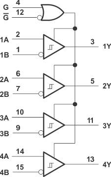
The AM26C32 device is a quadruple differential line receiver for balanced or unbalanced digital data transmission. The enable function is common to all four receivers and offers a choice of active-high or active-low input. The 3-state outputs permit connection directly to a bus-organized system. Fail-safe design specifies that if the inputs are open, the outputs always are high. The AM26C32 devices are manufactured using a BiCMOS process, which is a combination of bipolar and CMOS transistors. This process provides the high voltage and current of bipolar with the low power of CMOS to reduce the power consumption to about one-fifth that of the standard AM26LS32, while maintaining AC and DC performance.
| PART NUMBER | PACKAGE(1) | PACKAGE SIZE(2) |
|---|---|---|
| AM26C32 | PDIP (N, 16) | 19.3 mm × 9.4 mm |
| SO (NS, 16) | 10.2 mm × 7.8 mm | |
| SOIC (D, 16) | 9.9 mm × 6 mm | |
| SSOP (DB, 16) | 6.2mm × 7.8mm | |
| TSSOP (PW, 16) | 5 mm × 6.4 mm | |
| CDIP (J, 16) | mm × 6.92 mm | |
| CFP (W, 16) | 10.3 mm × 6.73 mm | |
| LCCC (FK, 20) | 8.90 mm × 8.90 mm |
 Simplified Schematic