SLLS202H may 1995 – august 2023 AM26LV32
PRODUCTION DATA
- 1
- 1 Features
- 2 Applications
- 3 Description
- 4 Revision History
- 5 Pin Configuration and Functions
- 6 Specifications
- 7 Parameter Measurement Information
- 8 Detailed Description
- 9 Application and Implementation
- 10Device and Documentation Support
- 11Mechanical, Packaging, and Orderable Information
Package Options
Refer to the PDF data sheet for device specific package drawings
Mechanical Data (Package|Pins)
- NS|16
- D|16
Thermal pad, mechanical data (Package|Pins)
Orderable Information
8.3 Feature Description
The device can be configured using the G and G logic inputs to select receiver output. The high voltage or logic 1 on the G pin allows the device to operate on an active-high, and having a low voltage or logic 0 on the G enables active-low operation. These are simple ways to configure the logic to match that of the receiving or transmitting controller or microprocessor.
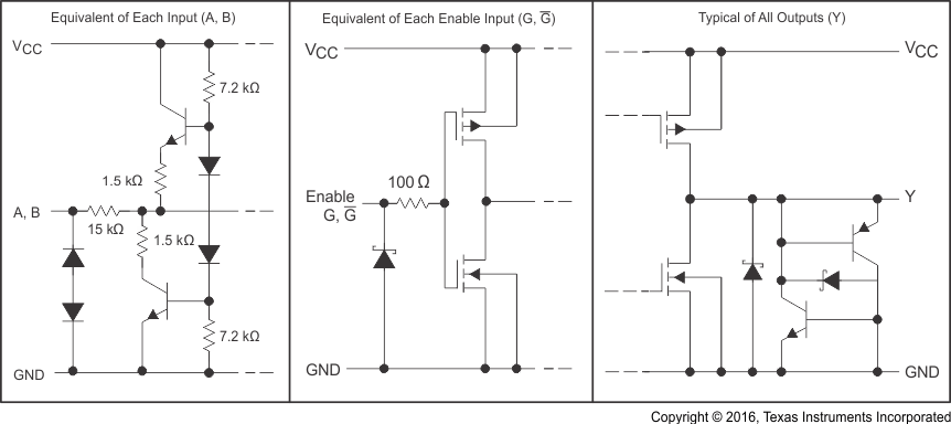
 Figure 8-2 Schematics of Equivalent Inputs and Outputs