SPRS550F October 2009 – July 2014 AM3505 , AM3517
PRODUCTION DATA.
- 1Device Summary
- 2Revision History
- 3Device Comparison
- 4Terminal Configuration and Functions
- 5Specifications
-
6Timing Requirements and Switching Characteristics
- 6.1 Timing Test Conditions
- 6.2 Interface Clock Specifications
- 6.3 Timing Parameters
- 6.4
External Memory Interfaces
- 6.4.1 General-Purpose Memory Controller (GPMC)
- 6.4.2
SDRAM Controller (SDRC)
- 6.4.2.1 LPDDR Interface
- 6.4.2.2
DDR2 Interface
- 6.4.2.2.1 DDR2 Interface Schematic
- 6.4.2.2.2 Compatible JEDEC DDR2 Devices
- 6.4.2.2.3 PCB Stackup
- 6.4.2.2.4 Placement
- 6.4.2.2.5 DDR2 Keep Out Region
- 6.4.2.2.6 Bulk Bypass Capacitors
- 6.4.2.2.7 High-Speed Bypass Capacitors
- 6.4.2.2.8 Net Classes
- 6.4.2.2.9 DDR2 Signal Termination
- 6.4.2.2.10 VREF Routing
- 6.4.2.2.11 DDR2 CLK and ADDR_CTRL Routing
- 6.4.2.2.12 On Die Termination (ODT)
- 6.5 Video Interfaces
- 6.6
Serial Communications Interfaces
- 6.6.1 Multichannel Buffered Serial Port (McBSP) Timing
- 6.6.2 Multichannel Serial Port Interface (McSPI) Timing
- 6.6.3 Multiport Full-Speed Universal Serial Bus (USB) Interface
- 6.6.4 Multiport High-Speed Universal Serial Bus (USB) Timing
- 6.6.5 USB0 OTG (USB2.0 OTG)
- 6.6.6 High-End Controller Area Network Controller (HECC) Timing
- 6.6.7 Ethernet Media Access Controller (EMAC)
- 6.6.8 Management Data Input/Output (MDIO)
- 6.6.9 Universal Asynchronous Receiver/Transmitter (UART)
- 6.6.10 HDQ / 1-Wire Interfaces
- 6.6.11 I2C Interface
- 6.7 Removable Media Interfaces
- 6.8 Test Interfaces
- 7Device and Documentation Support
- 8Mechanical Packaging and Orderable Information
Package Options
Refer to the PDF data sheet for device specific package drawings
Mechanical Data (Package|Pins)
- ZER|484
- ZCN|491
Thermal pad, mechanical data (Package|Pins)
Orderable Information
5 Specifications
5.1 Absolute Maximum Ratings
Table 5-1 specifies the absolute maximum ratings over the operating junction temperature range of commercial and extended temperature devices. Stresses beyond those listed under absolute maximum ratings may cause permanent damage to the device. These are stress ratings only and functional operation of the device at these or any other conditions beyond those indicated under recommended operating conditions is not implied. Exposure to absolute-maximum-rated conditions for extended periods may affect device reliability.
Notes:
- Logic functions and parameter values are not assured out of the range specified in the recommended operating conditions.
Table 5-1 Absolute Maximum Ratings Over Operating Junction Temperature Range
| PARAMETER | MIN | MAX | UNIT | ||
|---|---|---|---|---|---|
| VDD_CORE | Supply voltage range for core macros | -0.5 | 1.6 | V | |
| VDDS | Second supply voltage range for 1.8-V I/O macros | -0.5 | 2.25 | V | |
| VDDSHV | Supply voltage range for 1.8/3.3V I/O macros | -0.5 | 3.8 | V | |
| VDDS_SRAM_MPU | Analog Supply voltage range for 1.8-V MPU SLDO | -0.5 | 2.25 | V | |
| VDDS_SRAM_CORE_BG | Analog Supply voltage range for 1.8-V Core SLDO and VDDA of BandGap | -0.5 | 2.25 | V | |
| VDDS_DPLL_MPU_USBHOST | Analog power supply for 1.8-V MPUSS DPLL and USBHOST DPLL | -0.5 | 2.1 | V | |
| VDDS_DPLL_PER_CORE | Analog power supply for 1.8-V DPLL and HSDIVIDER/ CORE and HSDIVIDER | -0.5 | 2.1 | V | |
| VDDA_DAC | Analog Power Supply for 1.8-V DAC | -0.5 | 2.43 | V | |
| VDDA3P3V_USBPHY | Analog power supply for 3.3-V USB transceiver | -0.5 | 3.6 | V | |
| VDDA1P8V_USBPHY | Power Supply for 1.8-V USB transceiver | -0.5 | 2.0 | V | |
| VDDSOSC | Power Supply for 1.8-V oscillator | -0.5 | 2.1 | V | |
| VPAD | Voltage range at PAD | Oscillator input (sys_xtalin) | -0.3 | VDDSOSC + 0.3 | V |
| VDDS 1.8-V I/O macros | -0.3 | VDDS + 0.3 | |||
| Dual-voltage LVCMOS inputs, VDDSHV = 1.8 V | -0.3 | VDDSHV + 0.3 | |||
| Dual-voltage LVCMOS inputs, VDDSHV = 3.3 V | -0.3 | 3.8 | |||
| USB VBUS pin (usb0_vbus) | 5.5 | ||||
| USB 5V Tolerant IOs (usb0_dp, usb0_dm, usb0_id) | 5.25 | ||||
| IIOI | Current-pulse injection on each I/O pin(1) | 200 | mA | ||
| Iclamp | Clamp current for an input or output | -20 | 20 | mA | |
5.2 Handling Ratings
Table 5-2 Handling Ratings
| PARAMETER | MIN | MAX | UNIT | ||
|---|---|---|---|---|---|
| VESD | ESD stress voltage(1) | HBM (human body model)(2) | >1000 | V | |
| CDM (charged device model)(3) | >500 | ||||
| Tstg | Storage temperature range | -65 | 150 | °C | |
5.3 Recommended Operating Conditions
All AM3517/05 modules are used under the operating conditions contained in Table 5-3.
Note: Logic functions and parameter values are not assured if the device is operated out of the range specified in the recommended operating conditions.
Table 5-3 Recommended Operating Conditions
| PARAMETER | DESCRIPTION | MIN | NOM | MAX | UNIT | |
|---|---|---|---|---|---|---|
| VDD_CORE | Core and oscillator macros power supply | 1.152 | 1.20 | 1.248 | V | |
| Noise (peak-peak) | 24.00 | mVpp | ||||
| VDDS_SRAM_MPU | MPU SRAM LDO analog power supply | 1.71 | 1.80 | 1.89 | V | |
| Noise (peak-peak) | 50.00 | mVpp | ||||
| VDDS_SRAM_CORE_BG | Core SRAM LDO and BandGap analog power supply | 1.71 | 1.80 | 1.89 | V | |
| Noise (peak-peak) | 50.00 | mVpp | ||||
| VDDS_DPLL_MPU_ USBHOST |
MPU and USBHOST DPLL analog power supply | 1.71 | 1.80 | 1.89 | V | |
| Noise (peak-peak) | 35.00 | mVpp | ||||
| VDDS_DPLL_ PER_CORE |
Peripherals and Core DPLLs analog power supply | 1.71 | 1.80 | 1.89 | V | |
| Noise (peak-peak) | 35.00 | mVpp | ||||
| VDDA_DAC | DAC analog power supply | 1.71 | 1.80 | 1.89 | V | |
| Noise (peak-peak) | 30.00 | mVpp | ||||
| VSSA_DAC | DAC analog ground | 0.00 | V | |||
| VDDA3P3V_ USBPHY |
Analog power supply for 3.3-V USB transceiver | 3.14 | 3.30 | 3.47 | V | |
| Noise (peak-peak) | 70.00 | mVpp | ||||
| VDDA1P8V_ USBPHY |
Power Supply for 1.8-V USB transceiver | 1.71 | 1.80 | 1.89 | V | |
| Noise (peak-peak) | 50.00 | mVpp | ||||
| VDDSHV | 3.3-/1.8-V power supply | 1.8 V Mode | 1.71 | 1.80 | 1.89 | V |
| 3.3 V Mode | 3.14 | 3.30 | 3.47 | V | ||
| VDDS | 1.8-V power supply | 1.71 | 1.80 | 1.89 | V | |
| Tj | Operating junction temperature range | Commercial Temperature |
0 | 90 | °C | |
| Extended Temperature |
-40 | 105 | °C | |||
| Device Operating Life Power-On Hours (POH)(1) | 500 MHz ARM Clock Freq. | < 90°C TJ | 100K | hrs. | ||
| 90 - 105 °C TJ | 100K | |||||
| 600 MHz ARM Clock Freq. | < 90°C TJ | 100K | ||||
| 90 - 105 °C TJ | 50K(2) | |||||
Figure 5-1 shows the power domains:
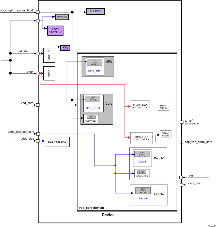 Figure 5-1 AM3517/05 Voltage Domains
5.4 Power Consumption Summary
The supply voltages and power consumption estimates are detailed in Table 5-4.
Table 5-4 Estimated Power Consumption at Ball Level
| SIGNAL NAME | DESCRIPTION | MAX CURRENT (mA) | |
|---|---|---|---|
| VDD_CORE | 1.2-V core and oscillator macros power supply | AM3517 | 1500 mA |
| AM3505 | 1400 mA | ||
| VDDS_SRAM_MPU | 1.8-V MPU SLDO analog power supply | 40 mA | |
| VDDS_SRAM_CORE_BG | 1.8-V Core SLDO and VDDA of BandGap analog power supply | 40 mA | |
| VDDS_DPLL_MPU_USBHOST | 1.8-V MPUSS DPLL and USBHOST DPLL analog power supply | 25 mA | |
| VDDS_DPLL_PER_CORE | 1.8-V DPLL and HSDIVIDER/ CORE and HSDIVIDER analog power supply | 25 mA | |
| VDDA_DAC | 1.8-V DAC analog power supply | 65 mA | |
| VDDA3P3V_USBPHY | 3.3-V USB transceiver analog power supply | 10 mA | |
| VDDA1P8V_USBPHY | 1.8-V USB transceiver power supply | 50 mA | |
| VDDSHV | 3.3-/1.8-V power supply | 300 mA | |
| VDDS | 1.8-V power supply | 200 mA | |
| VDDSOSC | 1.8-V oscillator power supply | 20 mA | |
5.5 Electrical Characteristics
Table 5-5 summarizes the DC electrical characteristics.
Table 5-5 DC Electrical Characteristics
| PARAMETER | MIN | NOM | MAX | UNIT | ||||
|---|---|---|---|---|---|---|---|---|
| LVCMOS Pin Buffers | ||||||||
| VIH | High-level input voltage | VDDSHV = 1.8 V(1) | 0.65 x VDDSHV. | V | ||||
| VDDSHV = 3.3 V(1) | 2 | |||||||
| sys_xtalin | 0.8 x VDDSOSC | |||||||
| VIL | Low-level input voltage | VDDSHV = 1.8 V(1) | 0.35 x VDDSHV | V | ||||
| VDDSHV = 3.3 V(1) | 0.8 | |||||||
| sys_xtalin | 0.2 x VDDSOSC | |||||||
| VOH | High-level output voltage | VDDSHV = 1.8 V(1)
IOH = -2 mA |
VDDSHV - 0.45 | V | ||||
| VDDSHV = 3.3 V(1)
IOH = -2 mA |
2.4 | |||||||
| VOL | Low-level output voltage | VDDSHV = 1.8 V(1)
IOL = 2 mA |
0.45 | V | ||||
| VDDSHV = 3.3 V(1)
IOL = 2 mA |
0.4 | |||||||
| II | Input current for dual voltage IO pins | VI = Vss to VDDSHV | Input pins with pull disabled | -9 | 9 | µA | ||
| VI = Vss to VDDSHV | Input pins with 100 µA pull-up enabled | -310 | -70 | |||||
| VI = Vss to VDDSHV | Input pins with 100 µA pull-down enabled | 75 | 270 | |||||
| Input current for DDR2/mDDR 1.8V IO pins | VI = Vss to VDDSHV | Input pins with 100 µA pull-down enabled | 77 | 286 | ||||
| IOZ | Off-state output current | VO = VDDSHV or 0V | Pull disabled | -20 | 20 | µA | ||
| IOH | High-level output current (dual-voltage LVCMOS IOs) | -2 | mA | |||||
| IOL | Low-level output current (dual-voltage LVCMOS IOs) | 2 | mA | |||||
| tT | Input transition time (rise time, tR or fall time, tF evaluated between 10% and 90% at PAD) | VDDSHV = 1.8 V(1) | Normal mode | 10 | ns | |||
| High-speed mode | 3 | |||||||
| VDDSHV = 3.3 V(1) | Normal mode | 10 | ||||||
| High-speed mode | 3 | |||||||
| Capacitance | Input capacitance (dual-voltage LVCMOS I/Os) |
3 | pF | |||||
| Output capacitance (dual-voltage LVCMOS I/Os) |
3 | pF | ||||||
| Complex IO Dedicated to USB : USB0_DM and USB0_DP | ||||||||
| VIH | High-level input voltage | Low/Full speed | 2.0 | V | ||||
| High speed | (2) | |||||||
| VIL | Low-level input voltage | Low/Full speed | 0.8 | V | ||||
| High speed | (2) | |||||||
| VOH | High-level output voltage | Low/Full speed | 2.8 | VDDA3P3V_ USBPHY |
V | |||
| High speed | 360 | 440 | mV | |||||
| VOL | Low-level output voltage | Low/Full speed | 0.0 | 0.3 | V | |||
| High speed | -10 | 10 | mV | |||||
5.6 Thermal Characteristics
Table 5-6 and Table 5-7 provide the thermal resistance characteristics for the recommended package types used on the AM3517/05.
Table 5-6 Package Thermal Resistance Characteristics [ZCN Package]
| NAME | DESCRIPTION | AIR FLOW (m/s)(1) | ZCN (°C/W)(2) |
|---|---|---|---|
| ΘJC | Junction-to-case (1S0P)(3) | NA | 2.6 |
| ΘJB | Junction-to-board (2S2P)(3) | NA | 10.1 |
| ΘJA | Junction-to-free air (2S2P)(3) | 0.0 | 24.1 |
| 1.0 | 18.7 | ||
| 2.0 | 17.5 | ||
| 3.0 | 16.8 | ||
| ΨJT | Junction-to-package top (2S2P)(3) | 0.0 | 0.05 |
| 1.0 | 0.2 | ||
| 2.0 | 0.2 | ||
| 3.0 | 0.3 | ||
| ΨJB | Junction-to-board (2S2P)(3) | 0.0 | 10.0 |
| 1.0 | 10.3 | ||
| 2.0 | 10.2 | ||
| 3.0 | 10.1 |
Table 5-7 Package Thermal Resistance Characteristics [ZER](4)
| NAME | DESCRIPTION | AIR FLOW (m/s)(1) | ZER (°C/W)(2) |
|---|---|---|---|
| ΘJC | Junction-to-case (2S2P)(3) | NA | 6 |
| ΘJB | Junction-to-board (2S2P)(3) | NA | 6 |
| ΘJA | Junction-to-free air (2S2P)(3) | 0.0 | 15.8 |
| 1.0 | 12.0 | ||
| 2.0 | 11.1 | ||
| 3.0 | 10.8 | ||
| ΨJT | Junction-to-package top (2S2P)(3) | 0.0 | 3.3 |
| 1.0 | 3.7 | ||
| 2.0 | 3.5 | ||
| 3.0 | 3.5 | ||
| ΨJB | Junction-to-board (2S2P)(3) | 0.0 | 6.0 |
| 1.0 | 6.1 | ||
| 2.0 | 5.8 | ||
| 3.0 | 5.7 |
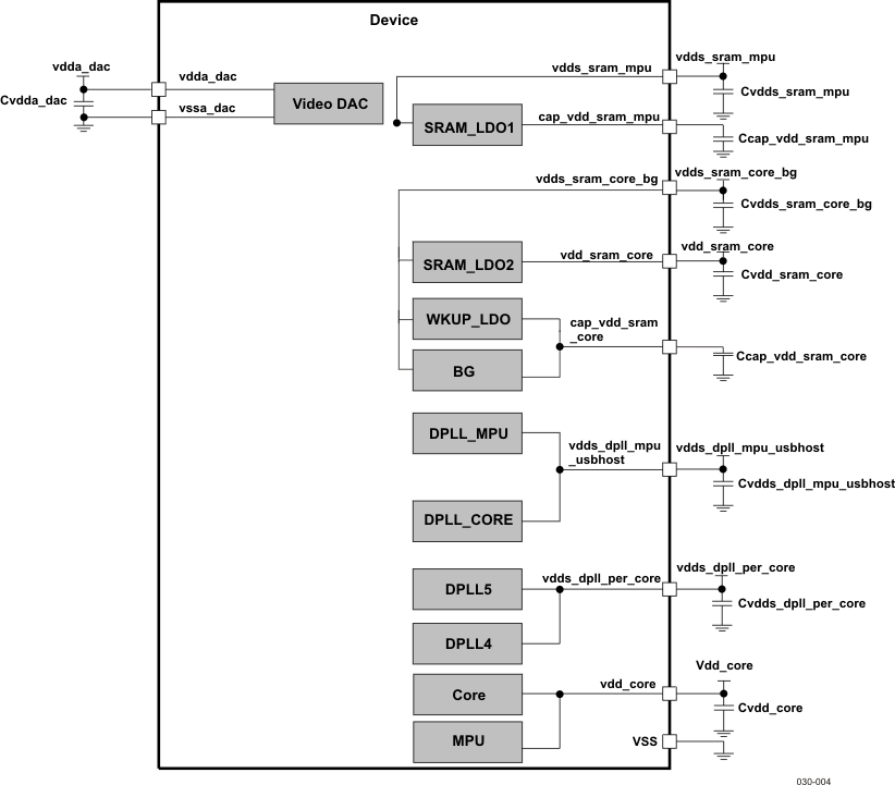
5.7 Core Voltage Decoupling
For module performance, decoupling capacitors are required to suppress the switching noise generated by high frequency and to stabilize the supply voltage. A decoupling capacitor is most effective when it is close to the device because this minimizes the inductance of the circuit board wiring and interconnects.
Table 5-8 summarizes the power supplies decoupling characteristics.
Table 5-8 Core Voltage Decoupling Characteristics
| PARAMETER | MIN | TYP | MAX | UNIT |
|---|---|---|---|---|
| Cvdd_core(1) | 50 | 100 | 120 | nF |
| Ccap_vdd_sram_core | 100 | nF | ||
| Cvdds_dpll_mpu_usbhost | 100 | nF | ||
| Cvdds_dpll_per_core | 100 | nF | ||
| Cvdda_dac | 100 | nF | ||
| Cvdd_sram_core | 100 | nF | ||
| Cvdd_sram_core_bg | 100 | nF | ||
| Cvdds_sram_mpu | 100 | nF | ||
| Cvddshv | 100 | nF | ||
| Cvdda3p3v_usbphy | 100 | nF | ||
| Cvdda1p8v_usbphy | 100 | nF |
Figure 5-2 shows an example of power supply decoupling.
5.8 Power-up and Power-down
This section provides the timing requirements for the AM3517/05 hardware signals.
5.8.1 Power-up Sequence
The following steps give an example of power-up sequence supported by the AM3517/05.
- IO 1.8V supply (VDDS), Band-gap and LDO supplies (VDDS_SRAM_CORE_BG, VDDS_SRAM_MPU) and oscillator supply (VDDSOSC) should come up first to a stable state.
- IO 3.3V (VDDSHV) supply should be ramped up next to a stable state.
- Core (VDD_CORE) supply follows next to a stable state.
- All the PLL supplies (VDDS_DPLL_PER_CORE, VDDS_DPLL_MPU_USBHOST) and 1.8 V complex IO supplies (VDDA_DAC, VDDA1P8V_USBPHY) should be ramped up next to a stable state.
- Finally, 3.3 V complex IO (VDDA_3P3V_USBPHY) should be ramped up.
- sys_nrespwron must be held low at the time the power supplies are ramped up till the time the sys_32k and sys_xtalin clocks are stable.
Note: In VDDSHV 1.8 V operation mode, VDDSHV can be grouped and powered up together with VDDS, VDDS_SRAM_CORE_BG, VDDS_SRAM_MPU and VDDSOSC.
Figure 5-3 shows the power-up sequence.
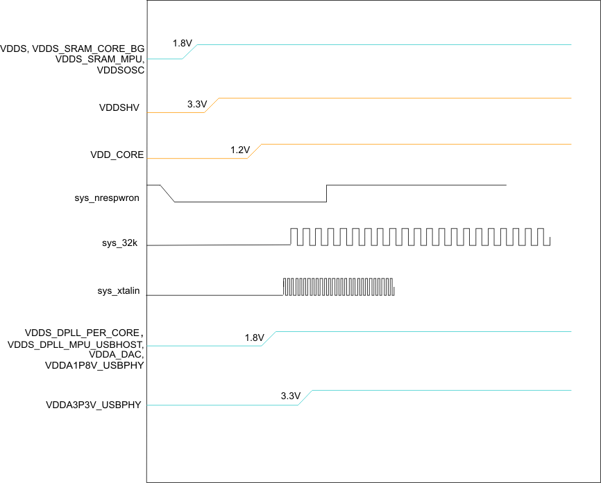 Figure 5-3 Power-up Sequence
5.8.2 Power-down Sequence
The AM3517/05 device proceeds with the power-down sequence shown below.
The following steps give an example of the power-down sequence supported by the AM3517/05 device.
- Reset AM3517/05 device.
- Stop all signals driven to AM3517/05.
- Option 1: Power down all domains simutaneously.
- Option 2: If all domains cannot be powered down simultaneously, follow the below sequence:
- Power off all complex I/O domains
- Power off core domain (VDD_CORE)
- Power off all PLL domains (VDDS_DPLL_MPU_USBHOST and VDDS_DPLL_PER_CORE)
- Power off all SRAM LDOs
- Power off all standard I/O domains (VDDS and VDDSHV)
5.9 Clock Specifications
The AM3517/05 device has three external input clocks, a low frequency (sys_32k), a high frequency (sys_xtalin), and an optional (sys_altclk). The AM3517/05 device has two configurable output clocks, sys_clkout1 and sys_clkout2.
Figure 5-4 shows the interface to the external clock sources and clock outputs.
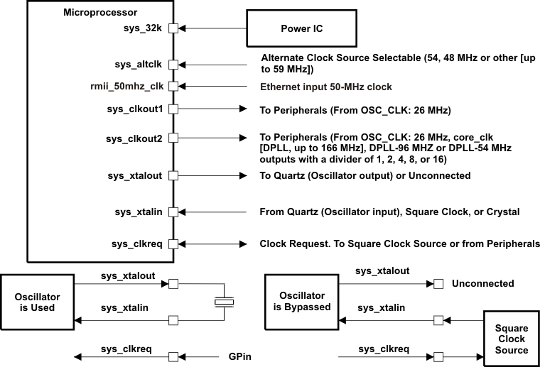 Figure 5-4 Clock Interface
The AM3517/05 device operation requires the following three input clocks:
- The 32-kHz clock can be generated using one of the following options and can be selected via the sys_boot7 pin. See Figure 5-5.
- External: Supplied by an oscillator on the sys_32k pin.
- Internal: 32-kHz clock generation using a fixed divider on the HS system clock (26MHz).
- The system alternative clock can be used (through the sys_altclk pin) to provide alternative 48 or 54 MHz or other clock source (up to 54 MHz).
- The system clock input (26 MHz) is used to generate the main source clock of the AM3517/05 device. It supplies the DPLLs as well as several AM3517/05 modules. The system clock input can be connected to either:
- A crystal oscillator clock managed by sys_xtalin and sys_xtalout. In this case, the sys_clkreq is used as an input (GPIN).
- A CMOS digital clock through the sys_xtalin pin. In this case, the sys_clkreq is used as an output to request the external system clock.
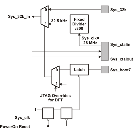 Figure 5-5 32-kHz Clock Generation
The AM3517/05 outputs externally two clocks:
- sys_clkout1 can output the oscillator clock (26 MHz) at any time.
- sys_clkout2 can output the oscillator clock, core_clk, 96 MHz or 54 MHz. It can be divided by 2, 4, 8, or 16 and its off state polarity is programmable.
5.9.1 Oscillator
The sys_xtalin (26 MHz) oscillator provides the primary reference clock for the device. The on-chip oscillator requires an external crystal connected across the sys_xtalin and sys_xtalout pins, along with two load capacitors, as shown in Figure 4-3. The external crystal load capacitors must be connected only to the oscillator ground pin (VSSOSC). Do not connect to board ground (VSS).
Note: If an external oscillator is to be used, the external oscillator clock signal should be connected to the sys_xtalin pin with a 1.8V amplitude. The sys_xtalout should be left unconnected and the VSSOSC signal should be connected to board ground (VSS).
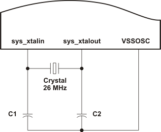
Table 5-9 Crystal Electrical Characteristics
| PARAMETER | MIN | TYP | MAX | UNIT |
|---|---|---|---|---|
| Oscillation frequency | 26 | MHz | ||
| Crystal ESR | 50 | Ω | ||
| Frequency stability | +/- 50 | ppm | ||
| Parallel Load Capacitance (C1 and C2) | 20 | pF | ||
| Shunt Capacitance | 5 | pF |
5.9.2 Input Clock Specifications
The clock system accepts three input clock sources:
- 32-kHz digital CMOS clock
- Crystal oscillator clock or CMOS digital clock (26 MHz)
- Alternate clock (48 or 54 MHz, or other up to 54 MHz)
Table 5-10 26-MHz SYS_CLK Input Clock Timing Requirements
| PARAMETER | DESCRIPTION | MIN | TYP | MAX | UNIT |
|---|---|---|---|---|---|
| f(xtalin) | Frequency, sys_xtalin | 26 | MHz | ||
| tw(xtalin) | Duty Cycle, sys_xtalin | 45 | 55 | % | |
| tj(xtalin) | Jitter, sys_xtalin | -1 | 1 | % | |
| tt(xtalin) | Transition time, sys_xtalin | 5 | ns | ||
Table 5-11 and Table 5-12 detail the electrical characteristics and input requirements of the 32-kHz input clock.
Table 5-11 32-kHz Input Clock Source Electrical Characteristics
| PARAMETER | DESCRIPTION | MIN | TYP | MAX | UNIT |
|---|---|---|---|---|---|
| f | Frequency, sys_32k | 32.768 | kHz | ||
| Ci | Input capacitance | 0.45 | pF | ||
| Ri | Input resistance | 0.25 | 106 | GΩ |
Table 5-12 32-kHz Input Clock Source Timing Requirements(1)
| PARAMETER | DESCRIPTION | MIN | TYP | MAX | UNIT |
|---|---|---|---|---|---|
| 1 / tc(32k) | Frequency, sys_32k | 32 | kHz | ||
| tR(32k) | Rise transition time, sys_32k | 20 | ns | ||
| tF(32k) | Fall transition time, sys_32k | 20 | ns | ||
| tJ(32k) | Frequency stability, sys_32k | +/-200 | ppm |
Table 5-13 and Table 5-14 detail the electrical characteristics and input requirements of the 48- or 54-MHz input clock.
Table 5-13 48-MHz, 54-MHz, or up to 59-MHz Input Clock Source Electrical Characteristics
| NAME | DESCRIPTION | MIN | MAX | UNIT |
|---|---|---|---|---|
| f | Frequency , sys_altclk | 48, 54, or up to 59 | MHz | |
| Ci | Input capacitance | 0.74 | pF | |
| Ri | Input resistance | 0.25 | 106 | GΩ |
Table 5-14 48-MHz, 54-MHz, or up to 59-MHz Input Clock Source Timing Requirements(1)(2)
| PARAMETER | DESCRIPTION | MIN | MAX | UNIT |
|---|---|---|---|---|
| 1 / tc(sys_altclk) | Frequency, sys_altclk | 48, 54, or up to 59 | MHz | |
| tw(sys_altclk) | Duty cycle | 45 | 60 | % |
| tj(sys_altclk) | Jitter | -1 | 1 | % |
| tr(sys_altclk) | Rise transition time | 10 | ns | |
| tf(sys_altclk) | Fall transition time | 10 | ns | |
| ft(sys_altclk) | Frequency tolerance | -50 | 50 | ppm |
5.9.3 Output Clock Specifications
Two output clocks (pin sys_clkout1 and pin sys_clkout2) are available:
- sys_clkout1 can output the oscillator clock (26 MHz) at any time. It can be controlled by software or externally using sys_clkreq control. When the device is in the off state, the sys_clkreq can be asserted to enable the oscillator and activate the sys_clkout1 without waking up the device. The off state polarity of sys_clkout1 is programmable.
- sys_clkout2 can output sys_clk (26 MHz), core_clk (core DPLL output), APLL-96 MHz, or APLL-54 MHz. It can be divided by 2, 4, 8, or 16 and its off state polarity is programmable. This output is active only when the core domain is active.
Table 5-15 summarizes the sys_clkout1 output clock electrical characteristics.
Table 5-15 SYS_CLKOUT1 Output Clock Electrical Characteristics
| NAME | DESCRIPTION | MIN | TYP | MAX | UNIT | |
|---|---|---|---|---|---|---|
| f | Frequency | 26 | MHz | |||
| CI | Load capacitance(1) | f(max) = 38.4 MHz | 70 | pF | ||
| f(max) = 26 MHz | 125 | |||||
Table 5-16 details the sys_clkout1 output clock timing characteristics.
Table 5-16 SYS_CLKOUT1 Output Clock Switching Characteristics
| NAME | DESCRIPTION | MIN | TYP | MAX | UNIT | |
|---|---|---|---|---|---|---|
| f | 1 / CO0 | Frequency | 26 | MHz | ||
| CO1 | tw(CLKOUT1) | Pulse duration, sys_clkout1 low or high | 0.40 * tc(CLKOUT1) |
0.60 * tc(CLKOUT1) |
ns | |
| CO2 | tR(CLKOUT1) | Rise time, sys_clkout1(1) | 3.31 | ns | ||
| CO3 | tF(CLKOUT1) | Fall time, sys_clkout1(1) | 3.31 | ns | ||
 Figure 5-6 SYS_CLKOUT1 System Output Clock
Table 5-17 summarizes the sys_clkout2 output clock electrical characteristics.
Table 5-17 SYS_CLKOUT2 Output Clock Electrical Characteristics
| NAME | DESCRIPTION | MIN | TYP | MAX | UNIT | |
|---|---|---|---|---|---|---|
| f | Frequency, sys_clkout2(2) | 166 | MHz | |||
| CL | Load capacitance(1) | f(max) = 166 MHz | 2 | 8 | 12 | pF |
Table 5-18 details the sys_clkout2 output clock timing characteristics.
Table 5-18 SYS_CLKOUT2 Output Clock Switching Characteristics
| NAME | DESCRIPTION | MIN | TYP | MAX | UNIT | |
|---|---|---|---|---|---|---|
| f | 1 / CO0 | Frequency | 166 | MHz | ||
| CO1 | tw(CLKOUT2) | Pulse duration, sys_clkout2 low or high | 0.40 * tc(CLKOUT2) | 0.60 * tc(CLKOUT2) | ns | |
| CO2 | tR(CLKOUT2) | Rise time, sys_clkout2(1) | 3.7 | ns | ||
| CO3 | tF(CLKOUT2) | Fall time, sys_clkout2(1) | 4.3 | ns | ||
 Figure 5-7 SYS_CLKOUT2 System Output Clock
5.9.4 DPLL Specifications
The AM3517/05 integrates four DPLLs. The PRM and CM drive them.
The four main DPLLs are:
- DPLL1 (MPU)
- DPLL3 (Core)
- DPLL4 (Peripherals)
- DPLL5 (Second Peripherals DPLL)
Figure 5-8 shows the DPLL implementation.
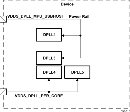 Figure 5-8 DPLL Implementation
5.9.4.1 Digital Phase-Locked Loop (DPLL)
The DPLL provides all interface clocks and some functional clocks (such as the processor clocks) of the AM3517/05 device.
DPLL1 gets an always-on clock used to produce the synthesized clock. They get a high-speed bypass clock used to switch the DPLL output clock on this high-speed clock during bypass mode.
The high-speed bypass clock is an L3 divided clock (programmable by 1 or 2) that saves DPLL processor power consumption when the processor does not need to run faster than the L3 clock speed, or optimizes performance during frequency scaling.
Each DPLL synthesized frequency is set by programming M (multiplier) and N (divider) factors. In addition, all DPLL outputs can be controlled by an independent divider (M2 to M6).
The clock generating DPLLs of the AM3517/05 device have following features:
- Independent power domain per DPLL
- Controlled by clock-manager (CM)
- Fed with always-on system clock with independent gating control per DPLL
- Analog part supplied through dedicated power supply (1.8 V) and an embedded LDO to get rid of 1-MHz noise
- Up to four independent output dividers for simultaneous generation of multiple clock frequencies
5.9.4.1.1 DPLL1 (MPU)
DPLL1 is located in the MPU subsystem and supplies all clocks of the subsystem. All MPU subsystem clocks are internally generated in the subsystem. When the core domain is on, it can use the DPLL3 (CORE DPLL) output as a high-frequency bypass input clock.
5.9.4.1.2 DPLL3 (CORE)
DPLL3 supplies all interface clocks and also a few module functional clocks. It can be also source of the emulation trace clock. It is located in the core domain area. All interface clocks and a few module functional clocks are generated in the CM. When the core domain is on, it can be used as a bypass input to DPLL1.
5.9.4.1.3 DPLL4 (Peripherals)
DPLL4 generates clocks for the peripherals. It supplies five clock sources: 96-MHz functional clocks to subsystems and peripherals, 54 MHz to TV DAC, display functional clock, camera sensor clock, and emulation trace clock. It is located in the core domain area. All interface clocks and few module functional clocks are generated in the CM. Its outputs to the DSS, PER, and EMU domains are propagated with always-on clock trees.
5.9.4.1.4 DPLL5 (Second peripherals DPLL)
DPLL5 supplies the 120-MHz functional clock to the CM.
5.9.4.2 DPLL Noise Isolation
The DPLL requires dedicated power supply pins to isolate the core analog circuit from the switching noise generated by the core logic that can cause jitter on the clock output signal. Guard rings are added to the cell to isolate it from substrate noise injection.
The vdd supplies are the most sensitive to noise; decoupling capacitance is recommended below the supply rails. The maximum input noise level allowed is 30 mVPP for frequencies below 1 MHz.
Figure 5-9 shows an example of a noise filter.
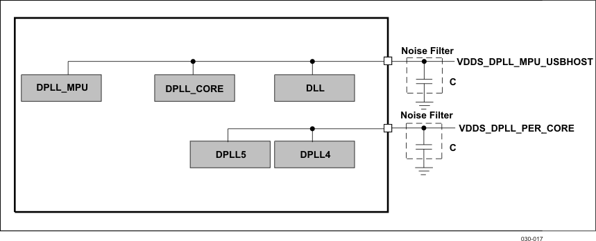 Figure 5-9 DPLL Noise Filter
Table 5-19 specifies the noise filter requirements.
Table 5-19 DPLL Noise Filter Requirements
| NAME | MIN | TYP | MAX | UNIT |
|---|---|---|---|---|
| Filtering capacitor | 100 | nF |
- The capacitors must be inserted between power and ground as close as possible.
- This circuit is provided only as an example.
- The filter must be located as close as possible to the device.
- No filtering required if noise is below 10 mVPP.
5.10 Video DAC Specifications
A dual-display interface equips the AM3517/05 processor. This display subsystem provides the necessary control signals to interface the memory frame buffer directly to the external displays (TV-set). Two (one per channel) 10-bit current steering DACs are inserted between the DSS and the TV set to generate the video analog signal. One of the video DACs also includes TV detection and power-down mode. Figure 5-10 shows the AM3517/05 DAC architecture.
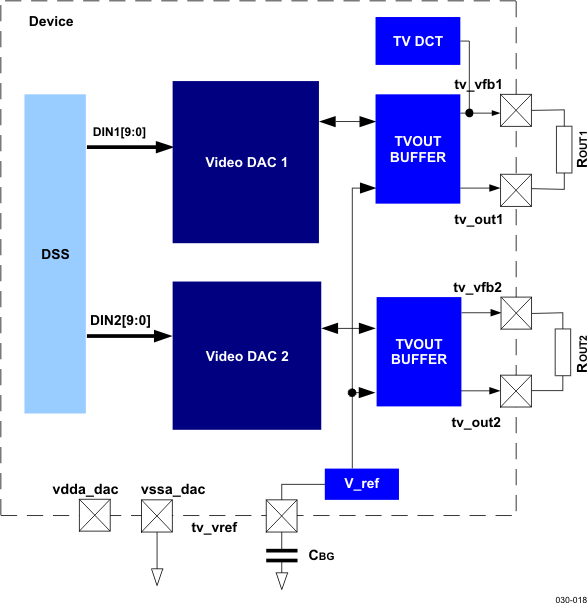 Figure 5-10 Video DAC Architecture
The following paragraphs detail the 10-bit DAC interface pinout, static and dynamic specifications, and noise requirements. The operating conditions and absolute maximum ratings are detailed in Table 5-21 and Table 5-23.
5.10.1 Interface Description
Table 5-20 summarizes the external pins of the video DAC.
Table 5-20 External Pins of 10-bit Video DAC
| PIN NAME | I/O | DESCRIPTION | |
|---|---|---|---|
| tv_out1 | O | TV analog output composite | DAC1 video output. An external resistor is connected between this node and tv_vfb1. The nominal value of ROUT1 is 1650 . Finally, note that this is the output node that drives the load (75 ). |
| tv_out2 | O | TV analog output S-VIDEO | DAC2 video output. An external resistor is connected between this node and tv_vfb2. The nominal value of ROUT2 is 1650 . Finally, note that this is the output node that drives the load (75 ). |
| tv_vref | I | Reference output voltage from internal bandgap | A decoupling capacitor (CBG) needs to be connected for optimum performance. |
| tv_vfb1 | O | Amplifier feedback node | Amplifier feedback node. An external resistor is connected between this node and tv_out1. The nominal value of ROUT1 is 1650 (1%). |
| tv_vfb2 | O | Amplifier feedback node | Amplifier feedback node. An external resistor is connected between this node and tv_out2. The nominal value of ROUT2 is 1650 (1%). |
5.10.2 Electrical Specifications Over Recommended Operating Conditions
(TMIN to TMAX, vdda_dac = 1.8 V, ROUT1/2 = 1650Ω , RLOAD = 75Ω , unless otherwise noted)
Table 5-21 DAC Static Electrical Specification
| PARAMETER | CONDITIONS/ASSUMPTIONS | MIN | TYP | MAX | UNIT | |
|---|---|---|---|---|---|---|
| R | Resolution | 10 | Bits | |||
| DC ACCURACY | ||||||
| INL(1) | Integral nonlinearity | 1 | 1 | LSB | ||
| DNL(2) | Differential nonlinearity | 1 | 1 | LSB | ||
| ANALOG OUTPUT | ||||||
| - | Full-scale output voltage | RLOAD = 75Ω | 0,7 | 0.88 | 1 | V |
| - | Output offset voltage | 50 | mV | |||
| - | Output offset voltage drift | 20 | mV/C | |||
| - | Gain error | 17 | 19 | % FS | ||
| RVOUT | Output impedance | 67.5 | 75 | 82.5 | ||
| REFERENCE | ||||||
| VREF | Reference voltage range | 0.525 | 0.55 | 0.575 | V | |
| - | Reference noise density | 100-kHz reference noise bandwidth | 129 | |||
| RSET | Full-scale current adjust resistor | 3700 | 4000 | 4200 | ||
| PSRR | Reference PSRR(3) (Up to 6 MHz) | 40 | dB | |||
| POWER CONSUMPTION | ||||||
| Ivdda-up | Analog Supply Current(4) | 2 channels, no load | 8 | mA | ||
| - | Analog supply driving a 75- load (RMS) | 2 channels | 50 | mA | ||
| Ivdda-up (peak) | Peak analog supply current: | Lasts less than 1 ns | 60 | mA | ||
| Ivdd-up | Digital supply current(5) | Measured at fCLK = 54 MHz, fOUT = 2 MHz sine wave, vdd = 1.3 V | 2 | mA | ||
| Ivdd-up (peak) | Peak digital supply current(6) | Lasts less than 1 ns | 2.5 | mA | ||
| Ivdda-down | Analog power at power-down | T = 30C, vdda = 1.8 V | 1.5 | mA | ||
| Ivdd-down | Digital power at power-down | T = 30C, vdd = 1.3 V | 1 | mA | ||
(TMIN to TMAX, vdda_dac = 1.8 V, ROUT1/2 = 1650 , RLOAD = 75 , unless otherwise noted)
Table 5-22 Video DAC Dynamic Electrical Specification
| PARAMETER | CONDITIONS/ASSUMPTIONS | MIN | TYP | MAX | UNIT | |
|---|---|---|---|---|---|---|
| fCLK(1) | Output update rate | Equal to input clock frequency | 54 | MHz | ||
| Clock jitter | rms clock jitter required in order to assure 10-bit accuracy | 40 | ps | |||
| Attenuation at 5.1 MHz | Corner frequency for signal | 0.1 | 0.5 | 1.5 | dB | |
| Attenuation at 54 MHz(1) | Image frequency | 25 | 30 | 33 | dB | |
| tST | Output settling time | Time from the start of the output transition to output within 1 LSB of final value. | 85 | ns | ||
| tRout | Output rise time | Measured from 10% to 90% of full-scale transition | 25 | ns | ||
| tFout | Output fall time | Measured from 10% to 90% of full-scale transition | 25 | ns | ||
| BW | Signal bandwidth | 6 | MHz | |||
| Differential gain(2) | 1.5% | |||||
| Differential phase(2) | 1 | deg. | ||||
| SFDR | Within bandwidth | fCLK = 54 MHz, fOUT = 1 MHz | 45 | dB | ||
| SNR | Signal-to-noise ratio 1 kHz to 6 MHz bandwidth |
fCLK = 54 MHz, fOUT = 1 MHz | 55(3) | dB | ||
| PSRR | Power supply rejection ratio | Up to 6 MHz | 20(4) | dB | ||
| Crosstalk | Between the two video channels | 50 | 40 | dB | ||
5.10.3 Analog Supply (vdda_dac) Noise Requirements
In order to assure 10-bit accuracy of the DAC analog output, the analog supply vdda_dac has to meet the noise requirements stated in this section.
The DAC Power Supply Rejection Ratio is defined as the relative variation of the full-scale output current divided by the supply variation. Thus, it is expressed in percentage of Full-Scale Range (FSR) per volt of supply variation as shown in the following equation: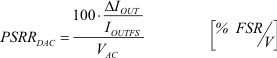
Depending on frequency, the PSRR is defined in Table 5-23.
Table 5-23 Video DAC Power Supply Rejection Ratio
| Supply Noise Frequency | PSRR % FSR/V |
|---|---|
| 0 to 100 kHz | 1 |
| > 100 kHz | The rejection decreases 20 dB/dec. Example: at 1 MHz the PSRR is 10% of FSR/V |
A graphic representation is shown in Figure 5-11.
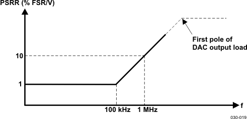 Figure 5-11 Video DAC Power Supply Rejection Ratio
To ensure that the DAC SFDR specification is met, the PSRR values and the clock jitter requirements translate to the following limits on vdda_dac (for the Video DAC).
The maximum peak-to-peak noise on vdda (ripple) is defined in Table 5-24:
Table 5-24 Video DAC Maximum Peak-to-Peak Noise on vdda_dac
| Tone Frequency | Maximum Peak-to-Peak Noise on vdda_dac |
|---|---|
| 0 to 100 kHz | < 30 mVpp |
| > 100 kHz | Decreases 20 dB/dec. Example: at 1 MHz the maximum is 3 mVpp |
The maximum noise spectral density (white noise) is defined in Table 5-25:
Table 5-25 Video DAC Maximum Noise Spectral Density
| Supply Noise Bandwidth | Maximum Supply Noise Density |
|---|---|
| 0 to 100 kHz | < 20 V / Hz |
| > 100 kHz | Decreases 20 dB/dec. Example: at 1 MHz the maximum noise density is 2 / Hz |
Because the DAC PSRR deteriorates at a rate of 20 dB/dec after 100 kHz, it is highly recommended to have vdda_dac low pass filtered (proper decoupling) (see the illustrated application: Section 5.10.4, External Component Value Choice).
5.10.4 External Component Value Choice
The full-scale output voltage VOUTMAX is regulated by the reference amplifier, and is set by an internal resistor RSET. IOUTMAX can be expressed as:
Where:
The output current IOUT appearing at DAC output is a function of both the input code and IOUTMAX and can be expressed as:
Where:
The output voltage is:
Where:
The TV-out buffer requires a per channel external resistors: ROUT1/2. The equation below can be used to select different resistor values (if necessary):
Recommended parameter values are:
Table 5-26 Video DAC Recommended External Components Values
| Recommended Value | UNIT | |
|---|---|---|
| CBG | 100 | nF |
| ROUT1/2 | 1650 | Ω |
In order to limit the reference noise bandwidth and to suppress transients on VREF, it is necessary to connect a large decoupling capacitor ©BG) between the tv_vref and vssa_dac pins.