SBAS585A September 2012 – January 2016 AMC1200-Q1
PRODUCTION DATA.
- 1 Features
- 2 Applications
- 3 Description
- 4 Revision History
- 5 Pin Configurations and Functions
- 6 Specifications
- 7 Detailed Description
- 8 Application and Implementation
- 9 Power Supply Recommendations
- 10Layout
- 11Device and Documentation Support
- 12Mechanical, Packaging, and Orderable Information
Package Options
Mechanical Data (Package|Pins)
Thermal pad, mechanical data (Package|Pins)
- DUB|8
Orderable Information
7 Detailed Description
7.1 Overview
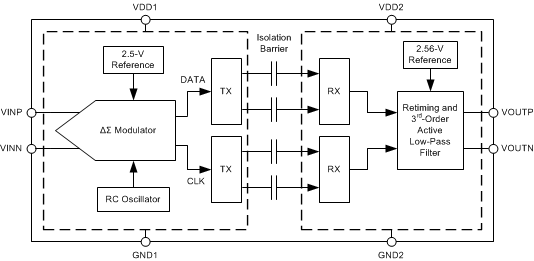
The AMC1200-Q1 is a fully-differential precision isolation amplifier. The input stage of the device consists of a second-order, delta-sigma (ΔΣ) modulator, voltage reference, clock generator, and drivers for the capacitive isolation barrier. The modulator converts the analog input signal to the digital domain. The drivers transfer the output of the modulator and the clock signal across the isolation barrier that separates the high- and low-voltage domains. The received bitstream and clock signals are synchronized and processed by a third-order analog filter with a nominal gain of 8 on the low-side and presented as a differential output of the device, as shown in the Functional Block Diagram section.
The SiO2-based capacitive isolation barrier supports a high level of magnetic field immunity, as described in application report, ISO72x Digital Isolator Magnetic-Field Immunity (SLLA181). The digital modulation used in the AMC1200-Q1 and the isolation barrier characteristics result in high reliability and common-mode transient immunity.
7.2 Functional Block Diagram

7.3 Feature Description
7.3.1 Insulation Characteristics
over recommended operating conditions (unless otherwise noted)
| PARAMETER | TEST CONDITIONS | MIN | TYP | MAX | UNIT | ||
|---|---|---|---|---|---|---|---|
| VIORM | Maximum working insulation voltage | 1200 | VPEAK | ||||
| VPR | Input to output test voltage | Qualification test: after input/output safety test subgroup 2/3, VPR = VIORM × 1.2, t = 10 s, partial discharge < 5 pC |
1440 | VPEAK | |||
| Qualification test: method a, after environmental tests subgroup 1, VPR = VIORM × 1.6, t = 10 s, partial discharge < 5 pC |
1920 | ||||||
| 100% production test: method b1, VPR = VIORM × 1.875, t = 1 s, partial discharge < 5 pC |
2250 | ||||||
| VIOTM | Transient overvoltage | Qualification test: t = 60 s | 4250 | VPEAK | |||
| VISO | Insulation voltage per UL | Qualification test: VTEST = VISO, t = 60 s | 4250 | VPEAK | |||
| 100% production test: VTEST = 1.2 × VISO, t = 1 s | 5100 | ||||||
| RS | Insulation resistance | VIO = 500 V at TS | > 109 | Ω | |||
| PD | Pollution degree | 2 | |||||
Table 1. IEC 61000-4-5 Ratings
| PARAMETER | TEST CONDITIONS | VALUE | UNIT | |
|---|---|---|---|---|
| Surge immunity | 1.2-μs and 50-μs voltage surge or 8-μs and 20-μs current surge | ±6000 | V | |
Table 2. IEC 60664-1 Ratings
| PARAMETER | TEST CONDITIONS | SPECIFICATION |
|---|---|---|
| Basic isolation group | Material group | II |
| Installation classification | Rated mains voltage ≤ 150 VRMS | I-IV |
| Rated mains voltage ≤ 300 VRMS | I-IV | |
| Rated mains voltage ≤ 400 VRMS | I-III | |
| Rated mains voltage < 600 VRMS | I-III |
7.3.2 IEC Safety Limiting Values
Safety limiting intends to minimize potential damage to the isolation barrier upon failure of input or output (I/O) circuitry. A failure of the I/O circuitry can cause low resistance to ground or the supply and, without current limiting, dissipate sufficient power to overheat the die and damage the isolation barrier, potentially leading to secondary system failures.
| PARAMETER | TEST CONDITIONS | MIN | TYP | MAX | UNIT | |
|---|---|---|---|---|---|---|
| IS | Safety input, output, or supply current | θJA = 246°C/W, VIN = 5.5 V, TJ = 150°C, TA = 25°C | –10 | 10 | mA | |
| TC | Maximum case temperature | 150 | °C | |||
The safety-limiting constraint is the maximum junction temperature specified in the Absolute Maximum Ratings table. The power dissipation and junction-to-air thermal impedance of the device installed in the application hardware determine the junction temperature. The assumed junction-to-air thermal resistance in the Thermal Information table is that of a device installed in the JESD51-3, Low Effective Thermal Conductivity Test Board for Leaded Surface Mount Packages and is conservative. The power is the recommended maximum input voltage times the current. The junction temperature is then the ambient temperature plus the power times the junction-to-air thermal resistance.
7.3.3 Package Characteristics
Creepage and clearance requirements should be applied according to the specific equipment isolation standards of a specific application. Take care to maintain the creepage and clearance distance of the board design to ensure that the mounting pads of the isolator on the printed-circuit-board (PCB) do not reduce this distance. Creepage and clearance on a PCB become equal according to the measurement techniques shown in the TI Isolation Glossary. Techniques such as inserting grooves and/or ribs on the PCB are used to help increase these specifications.
7.3.4 Regulatory Information
| VDE/IEC | UL |
|---|---|
| Certified according to VDE V 0884-10 | Recognized under 1577 component recognition program |
| Certificate number: 40016131 | File number: E181974 |
7.3.5 Analog Input
The analog input voltage range (VIN = VVINP – VVINN) is tailored to directly accommodate a voltage drop across a shunt resistor used for current sensing. Note that there are two restrictions on the analog input signals. If the absolute input voltage on either VINP or VINN exceeds the absolute maximum range of GND1 – 0.5 V to VDD1 + 0.5 V, the input current must be limited to 10 mA to prevent damage of the integrated input protection diodes. In addition, the linearity and the noise performance of the device are ensured only when the differential analog input voltage remains within ±250 mV.
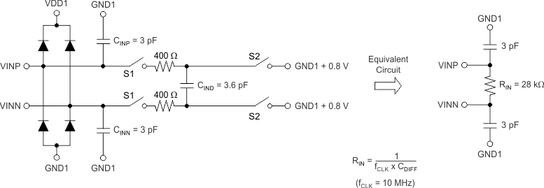
The differential analog input of the AMC1200-Q1 is a switched-capacitor circuit based on a second-order modulator stage that digitizes the input signal into a 1-bit output stream. The device compares the differential input signal VIN against the internal 2.5-V reference using internal capacitors that are continuously charged and discharged with a typical frequency of 10 MHz. With the S1 switches closed, CID charges to the voltage difference across VINP and VINN. For the discharge phase, both S1 switches open first and then both S2 switches close. CID discharges to approximately GND1 + 0.8 V during this phase. Figure 31 shows the simplified equivalent input circuitry.
 Figure 31. Equivalent Input Circuit
7.4 Device Functional Modes
The AMC1200-Q1 is operational when the power supplies VDD1 and VDD2 are applied as specified in the Recommended Operating Conditions section. The AMC1200-Q1 does not have any additional functional modes.