SBAS585A September 2012 – January 2016 AMC1200-Q1
PRODUCTION DATA.
- 1 Features
- 2 Applications
- 3 Description
- 4 Revision History
- 5 Pin Configurations and Functions
- 6 Specifications
- 7 Detailed Description
- 8 Application and Implementation
- 9 Power Supply Recommendations
- 10Layout
- 11Device and Documentation Support
- 12Mechanical, Packaging, and Orderable Information
Package Options
Mechanical Data (Package|Pins)
Thermal pad, mechanical data (Package|Pins)
- DUB|8
Orderable Information
8 Application and Implementation
NOTE
Information in the following applications sections is not part of the TI component specification, and TI does not warrant its accuracy or completeness. TI’s customers are responsible for determining suitability of components for their purposes. Customers should validate and test their design implementation to confirm system functionality.
8.1 Application Information
The AMC1200-Q1 offers unique linearity, high input common-mode rejection, low dc errors, and low temperature drift. These features make the AMC1200-Q1 a robust, high-performance isolation amplifier for automotive applications where high voltage isolation is required.
8.2 Typical Applications
8.2.1 Traction Inverter
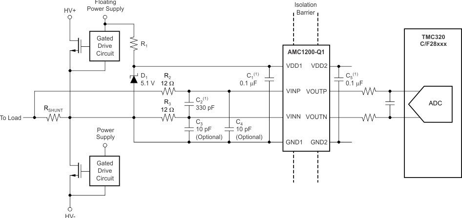
Figure 32 shows a typical operation of the AMC1200-Q1 for current sensing in a traction inverter application. Measurement of the phase current is done through the shunt resistor, RSHUNT (in this case, a two-pin shunt). The differential input and the high common-mode transient immunity of the AMC1200-Q1 ensure reliable and accurate operation even in high-noise environments (such as the power stage of the traction inverter).

Additionally, the AMC1200-Q1 can also be used for isolated voltage measurement of the dc-link as described in the Isolated Voltage Measurement section.
8.2.1.1 Design Requirements
Table 3 lists the parameters for the typical application in Figure 32.
Table 3. Design Requirements
| PARAMETER | VALUE | |
|---|---|---|
| High-side supply voltage | 5 V | |
| Low-side supply voltage | 3 V, or 3.3 V, or 5 V | |
| Voltage drop across shunt for linear response | ±250 mV (max) | |
8.2.1.2 Detailed Design Procedure
The high-side power supply (VDD1) for the AMC1200-Q1 is derived from the power supply of the upper gate driver. Further details are provided in the Power Supply Recommendations section.
The floating ground reference (GND1) is derived from one of the ends of the shunt resistor that is connected to the negative input of the AMC1200-Q1 (VINN). If a four-pin shunt is used, the inputs of the AMC1200-Q1 are connected to the inner leads and GND1 is connected to one of the outer shunt leads.
Use Ohm's Law to calculate the voltage drop across the shunt resistor (VSHUNT) for the desired current to be measured: VSHUNT = I × RSHUNT.
Consider the following two restrictions to choose the proper value of the shunt resistor RSHUNT:
- The voltage drop caused by the nominal current range must not exceed the recommended differential input voltage range: VSHUNT ≤ ±250 mV
- The voltage drop caused by the maximum allowed overcurrent must not exceed the input voltage that causes a clipping output: VSHUNT ≤ VClipping
For best performance, use an RC filter (components R2, R3, and C2 in Figure 32) to limit the noise bandwidth of the differential input signal. Limiting the value of resistors R2 and R3 to less than 24 Ω is recommended to avoid incomplete settling of the AMC1200-Q1 input circuitry (see Analog Input).
Optionally, the common-mode capacitors C3 and C4 can be used to reduce charge dumping from the inputs. Mismatch in values of C3 and C4 leads to a common-mode error at the modulator input. In this case, choose the value of the differential filter capacitor C2 to be at least 10 times larger than the values of C3 and C4 to limit the effect of the common-mode error. NP0-type capacitors are recommended to be used for C2, C3 and C4.
The differential output of the AMC1200-Q1 can either directly drive an analog-to-digital converter (ADC) input or can be further filtered before being processed by an ADC. For more information on the general procedure to design the filtering and driving stages for SAR ADCs, consult the TI Precision Designs 18 bit, 1Msps Data Acquisition Block Optimized for Lowest Distortion and Noise (SLAU515), and 18 bit Data Acquisition Block Optimized for Lowest Power (SLAU513) available for download at www.ti.com.
8.2.1.3 Application Curves
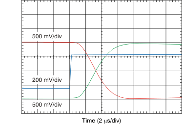
In traction inverter applications, the power switches must be protected in case of an overcurrent condition. To allow fast powering off of the system, a low delay caused by the isolation amplifier is required. Figure 33 shows the typical full-scale step response of the AMC1200-Q1.
The high linearity of the AMC1200-Q1, as shown in Figure 34, allows design of traction inverters with low torque ripple.


8.2.2 Isolated Voltage Measurement
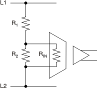
The AMC1200-Q1 can also be used for isolated voltage measurement applications, as shown in a simplified way in Figure 35. In such applications, usually a resistor divider (as conceptually indicated by R1 and R2) is used to scale the voltage amplitude. Choose the value of R2 to match the maximum voltage to be measured to the differential input voltage range VIN of the device. R2 and the input resistance RIN of the AMC1200-Q1 also create a resistance divider that results in additional gain error. With the assumption that R1 and RIN have a considerably higher value than R2, the resulting total gain error can be estimated using Equation 1:

where
- GERR = the gain error of the AMC1200-Q1
 Figure 35. Voltage Measurement Application