SBAS799 February 2017 AMC1304L05-Q1 , AMC1304L25-Q1 , AMC1304M05-Q1 , AMC1304M25-Q1
PRODUCTION DATA.
- 1 Features
- 2 Applications
- 3 Description
- 4 Revision History
- 5 Device Comparison Table
- 6 Pin Configurations and Functions
-
7 Specifications
- 7.1 Absolute Maximum Ratings
- 7.2 ESD Ratings
- 7.3 Recommended Operating Conditions
- 7.4 Thermal Information
- 7.5 Power Ratings
- 7.6 Insulation Specifications
- 7.7 Safety-Related Certifications
- 7.8 Safety Limiting Values
- 7.9 Electrical Characteristics: AMC1304x05-Q1
- 7.10 Electrical Characteristics: AMC1304x25-Q1
- 7.11 Switching Characteristics
- 7.12 Insulation Characteristics Curves
- 7.13 Typical Characteristics
- 8 Detailed Description
- 9 Application and Implementation
- 10Power-Supply Recommendations
- 11Layout
- 12Device and Documentation Support
- 13Mechanical, Packaging, and Orderable Information
Package Options
Mechanical Data (Package|Pins)
- DW|16
Thermal pad, mechanical data (Package|Pins)
- DW|16
Orderable Information
1 Features
- Qualified for Automotive Applications
- AEC-Q100 Qualified with the Following Results:
- Temperature Grade 1: –40°C to +125°C
- HBM ESD Classification Level 2
- CDM ESD Classification Level C6
-
Pin-Compatible Family with:
- ±50-mV or ±250-mV Input Voltage Ranges
- CMOS or LVDS Digital Interface Options
-
Excellent DC Performance:
- Offset Error: ±50 µV or ±100 µV (max)
- Offset Drift: 1.3 µV/°C (max)
- Gain Error: ±0.2% or ±0.3% (max)
- Gain Drift: ±40 ppm/°C (max)
- Safety-Related Certifications:
- 7000-VPK Reinforced Isolation per DIN V VDE V 0884-10 (VDE V 0884-10): 2006-12
- 5000-VRMS Isolation for 1 Minute per UL1577
- CAN/CSA No. 5A-Component Acceptance Service Notice
- Transient Immunity: 15 kV/µs (min)
- High Electromagnetic Field Immunity
(see Application Note SLLA181A) - External 5-MHz to 20-MHz Clock Input
- On-Chip 18-V LDO Regulator
2 Applications
- Shunt-Based Current Sensing or Resistor-Divider-Based Voltage Sensing In:
- Traction Inverters
- Onboard Chargers (OBC)
- DC-DC Converters
- Battery Management Systems (BMS)
3 Description
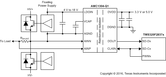
The AMC1304-Q1 is a precision, delta-sigma (ΔΣ) modulator with the output separated from the input circuitry by a capacitive double isolation barrier that is highly resistant to magnetic interference. This barrier is certified to provide reinforced isolation of up to 7000 VPEAK according to the DIN V VDE V 0884-10, UL1577 and CSA standards. Used in conjunction with isolated power supplies, the device prevents noise currents on a high common-mode voltage line from entering the local system ground and interfering with or damaging low voltage circuitry.
The input of the AMC1304-Q1 is optimized for direct connection to shunt resistors or other low voltage-level signal sources. The unique low input voltage range of the ±50-mV device allows significant reduction of the power dissipation through the shunt while supporting excellent ac and dc performance. By using an appropriate digital filter (that is, as integrated on the TMS320F2807x or TMS320F2837x families) to decimate the bit stream, the device can achieve 16 bits of resolution with a dynamic range of 81 dB (13.2 ENOB) at a data rate of 78 kSPS.
On the high-side, the modulator is supplied by an integrated low-dropout (LDO) regulator that allows an unregulated input voltage between 4 V and 18 V (LDOIN). The isolated digital interface operates from a 3.3-V or 5-V power supply (DVDD).
The AMC1304-Q1 is available in a wide-body SOIC-16 (DW) package.
Device Information(1)
| PART NUMBER | PACKAGE | BODY SIZE (NOM) |
|---|---|---|
| AMC1304x-Q1 | SOIC (16) | 10.30 mm × 7.50 mm |
- For all available packages, see the orderable addendum at the end of the datasheet.
Simplified Schematic
