SBASA51 May 2020 AMC1336-Q1
PRODUCTION DATA.
- 1 Features
- 2 Applications
- 3 Description
- 4 Revision History
- 5 Pin Configuration and Functions
-
6 Specifications
- Table 1. Absolute Maximum Ratings
- Table 2. ESD Ratings
- Table 3. Recommended Operating Conditions
- Table 4. Thermal Information
- Table 5. Power Ratings
- Table 6. Insulation Specifications
- Table 7. Safety-Related Certifications
- Table 8. Safety Limiting Values
- Table 9. Electrical Characteristics
- Table 10. Switching Characteristics
- 6.1 Insulation Characteristics Curves
- 6.2 Typical Characteristics
- 7 Detailed Description
- 8 Application and Implementation
- 9 Power Supply Recommendations
- 10Layout
- 11Device and Documentation Support
- 12Mechanical, Packaging, and Orderable Information
Package Options
Mechanical Data (Package|Pins)
- DWV|8
Thermal pad, mechanical data (Package|Pins)
Orderable Information
9 Power Supply Recommendations
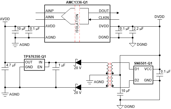
In a typical frequency-inverter application, the high-side power supply (AVDD) for the AMC1336-Q1 is generated from the controller-side supply (DVDD) of the device by an isolated dc/dc converter circuit. Figure 54 shows a low-cost solution based on the push-pull driver SN6501 and a transformer that supports the desired isolation voltage ratings. TI recommends using a low-ESR decoupling capacitor of 0.1 µF and an additional capacitor of minimum 1 µF for both supplies of the AMC1336-Q1. Place these decoupling capacitors as close as possible to the device power-supply pins to minimize supply current loops and electromagnetic emissions.
The AMC1336-Q1 does not require any specific power up sequencing. Consider the analog settling time tASTART as specified in the Table 10 table after ramp up of the AVDD high-side supply.
Connect the high-side ground pin AGND of the AMC1336-Q1 to one of the analog inputs AINx to avoid common-mode input voltage range violations.
 Figure 54. Decoupling the AMC1336-Q1