SBAS951B August 2019 – April 2020 AMC1336
PRODUCTION DATA.
- 1 Features
- 2 Applications
- 3 Description
- 4 Revision History
- 5 Pin Configuration and Functions
-
6 Specifications
- Table 1. Absolute Maximum Ratings
- Table 2. ESD Ratings
- Table 3. Recommended Operating Conditions
- Table 4. Thermal Information
- Table 5. Power Ratings
- Table 6. Insulation Specifications
- Table 7. Safety-Related Certifications
- Table 8. Safety Limiting Values
- Table 9. Electrical Characteristics
- Table 10. Switching Characteristics
- 6.1 Insulation Characteristics Curves
- 6.2 Typical Characteristics
- 7 Detailed Description
- 8 Application and Implementation
- 9 Power Supply Recommendations
- 10Layout
- 11Device and Documentation Support
- 12Mechanical, Packaging, and Orderable Information
Package Options
Mechanical Data (Package|Pins)
- DWV|8
Thermal pad, mechanical data (Package|Pins)
Orderable Information
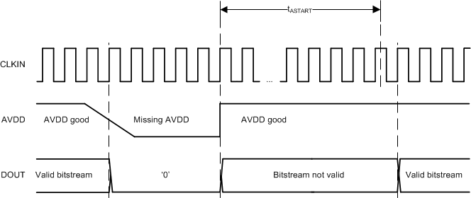
7.4.2 AVDD Diagnostics and Fail-Safe Output
In the case of a missing high-side supply voltage AVDD, the output of a ΔΣ modulator is not defined and can cause a system malfunction. In systems with high safety requirements, this behavior is not acceptable. As shown in Figure 49, the AMC1336 implements an AVDD diagnostics and fail-safe output function that ensures that the output DOUT of the device offers a steady-state bitstream of logic 0's in case of a missing AVDD. Sample at least 128 CLKIN cycles in order to distinguish a missing AVDD condition from an input underrange condition.
 Figure 49. Fail-Safe Output of the AMC1336